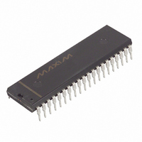
DS89C450-MNL+ Maxim Integrated Products, DS89C450-MNL+ Datasheet - Page 7

DS89C450-MNL+
Manufacturer Part Number
DS89C450-MNL+
Description
IC MCU FLASH 64KB 33MHZ 40-DIP
Manufacturer
Maxim Integrated Products
Series
89Cr
Datasheet
1.DS89C450-KIT.pdf
(46 pages)
Specifications of DS89C450-MNL+
Core Processor
8051
Core Size
8-Bit
Speed
33MHz
Connectivity
EBI/EMI, SIO, UART/USART
Peripherals
Power-Fail Reset, WDT
Number Of I /o
32
Program Memory Size
64KB (64K x 8)
Program Memory Type
FLASH
Ram Size
1K x 8
Voltage - Supply (vcc/vdd)
4.5 V ~ 5.5 V
Oscillator Type
External
Operating Temperature
-40°C ~ 85°C
Package / Case
40-DIP (0.600", 15.24mm)
Processor Series
89C
Core
8051
Data Bus Width
8 bit
Data Ram Size
1 KB
Maximum Clock Frequency
33 MHz
Number Of Programmable I/os
32
Number Of Timers
3
Maximum Operating Temperature
+ 85 C
Mounting Style
Through Hole
3rd Party Development Tools
PK51, CA51, A51, ULINK2
Development Tools By Supplier
DS89C450-K00
Minimum Operating Temperature
- 40 C
Interface Type
UART
Operating Supply Voltage
4.5 V to 5.5 V
Package
40PDIP
Device Core
8051
Family Name
89C
Maximum Speed
33 MHz
Lead Free Status / RoHS Status
Lead free / RoHS Compliant
Eeprom Size
-
Data Converters
-
Lead Free Status / Rohs Status
Lead free / RoHS Compliant
Note 16: External MOVX instruction times are dependent upon the setting of the MD2, MD1, and MD0 bits in the clock control register. The
Note 17: Maximum load capacitance (to meet the above timing) for Port 0, ALE, PSEN, WR, and RD is limited to 60pF. XTAL1 and XTAL2 load
Figure 1. Nonpage Mode Timing
Note 15: The clock divide and crystal multiplier control bits in the PMR register determine the system clock frequency and the minimum/
XTAL1
PSEN
Port 0
Port 2
ALE
RD
WR
MD2
4X/2X
0
0
0
0
1
1
1
1
terms “t
capacitance are dependent upon the frequency of the selected crystal.
X
X
X
1
0
maximum external clock speed. The term “1/t
following table. The minimum/maximum external clock speed columns clarify that [(external clock speed) x (multipliers)] cannot
exceed the rated speed of the device. In addition, the use of the crystal multiplier feature establishes a minimum external speed.
STC1
MD1
LSB
0
0
1
1
0
0
1
1
CD1
, t
0
0
0
1
1
STC2
MSB
t
LLIV
t
t
AVLL
AVLL2
, t
t
t
t
t
CLCL
t
STC3
PXIX
LLAX
PXIZ
LLPL
MD0
” used in the variable timing table above are calculated through the use of the table given below.
0
1
0
1
0
1
0
1
MOVX
CD0
0
0
1
0
1
MOVX Instruction Time
LSB
t
AVIV0
2 Machine Cycles
3 Machine Cycles
4 Machine Cycles
5 Machine Cycles
6 Machine Cycles
7 Machine Cycles
8 Machine Cycles
9 Machine Cycles
Number of External Clock
MSB
Cycles per System Clock
t
PLPH
t
AVWL2
MOVX
CLCL
t
Reserved
PLIV
(1/t
1024
” used in the AC Characteristics variable timing table is determined from the
1/4
1/2
1
CLCL
t
RLDV
)
t
DS89C430/DS89C450 Ultra-High-Speed Flash Micrcontrollers
LSB
t
AVDV2
AVDV0
7 of 46
MSB
t
t
AVLL3
LHLL
t
t
10 t
14 t
18 t
22 t
26 t
0 t
2 t
6 t
LLAX3
RLRH
t
STC1
CLCL
CLCL
CLCL
CLCL
CLCL
CLCL
CLCL
CLCL
DATA
t
LLDV
See AC Characteristics
See AC Characteristics
t
0 t
1 t
1 t
1 t
5 t
5 t
5 t
5 t
LSB
RHDX
t
t
STC2
t
AVIV2
CLCL
CLCL
CLCL
CLCL
CLCL
CLCL
CLCL
CLCL
RHDZ
10MHz
5MHz
Min
—
MSB
t
PLAZ
External Clock Speed
OPCODE
t
AVWL0
0 t
0 t
0 t
0 t
4 t
4 t
4 t
4 t
t
STC3
CLCL
CLCL
CLCL
CLCL
CLCL
CLCL
CLCL
CLCL
LSB
See AC Characteristics
See AC Characteristics
0 t
0 t
0 t
0 t
1 t
1 t
1 t
1 t
t
t
STC4
t
WHQX
t
CLCL
CLCL
CLCL
CLCL
CLCL
CLCL
CLCL
CLCL
WHLH
MSB
t
t
WLWH
8.25MHz
16.5MHz
LLAX2
LLWL
t
QVWX
Max
DATA
—
0 t
1 t
1 t
1 t
1 t
1 t
1 t
1 t
t
STC5
CLCL
CLCL
CLCL
CLCL
CLCL
CLCL
CLCL
CLCL


