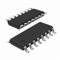
C8051F832-GS Silicon Laboratories Inc, C8051F832-GS Datasheet - Page 195

C8051F832-GS
Manufacturer Part Number
C8051F832-GS
Description
IC MCU 8BIT 4KB FLASH 16SOIC
Manufacturer
Silicon Laboratories Inc
Series
C8051F83xr
Datasheet
1.C8051F800DK.pdf
(250 pages)
Specifications of C8051F832-GS
Core Processor
8051
Core Size
8-Bit
Speed
25MHz
Connectivity
SMBus (2-Wire/I²C), SPI, UART/USART
Peripherals
POR, PWM, Temp Sensor, WDT
Number Of I /o
13
Program Memory Size
4KB (4K x 8)
Program Memory Type
FLASH
Ram Size
256 x 8
Voltage - Supply (vcc/vdd)
1.8 V ~ 3.6 V
Data Converters
A/D 12x10b
Oscillator Type
Internal
Operating Temperature
-40°C ~ 85°C
Package / Case
16-SOIC (3.9mm Width)
Processor Series
C8051F8x
Core
8051
Data Bus Width
16 bit
Data Ram Size
256 B
Interface Type
I2C, SPI, UART
Maximum Clock Frequency
25 MHz
Number Of Programmable I/os
13
Number Of Timers
3
Operating Supply Voltage
1.8 V to 3.6 V
Maximum Operating Temperature
+ 125 C
Mounting Style
SMD/SMT
3rd Party Development Tools
PK51, CA51, A51, ULINK2
Development Tools By Supplier
C8051F800DK
Minimum Operating Temperature
- 55 C
On-chip Adc
10 bit, 12 Channel
Lead Free Status / RoHS Status
Lead free / RoHS Compliant
Eeprom Size
-
Lead Free Status / Rohs Status
Details
Other names
336-1812-5
Available stocks
Company
Part Number
Manufacturer
Quantity
Price
Company:
Part Number:
C8051F832-GS
Manufacturer:
Silicon Labs
Quantity:
135
Company:
Part Number:
C8051F832-GSR
Manufacturer:
INTEL
Quantity:
101
- Current page: 195 of 250
- Download datasheet (2Mb)
26.5.3. Write Sequence (Slave)
During a write sequence, an SMBus master writes data to a slave device. The slave in this transfer will be
a receiver during the address byte, and a receiver during all data bytes. When slave events are enabled
(INH = 0), the interface enters Slave Receiver Mode when a START followed by a slave address and direc-
tion bit (WRITE in this case) is received. If hardware ACK generation is disabled, upon entering Slave
Receiver Mode, an interrupt is generated and the ACKRQ bit is set. The software must respond to the
received slave address with an ACK, or ignore the received slave address with a NACK. If hardware ACK
generation is enabled, the hardware will apply the ACK for a slave address which matches the criteria set
up by SMB0ADR and SMB0ADM. The interrupt will occur after the ACK cycle.
If the received slave address is ignored (by software or hardware), slave interrupts will be inhibited until the
next START is detected. If the received slave address is acknowledged, zero or more data bytes are
received.
If hardware ACK generation is disabled, the ACKRQ is set to 1 and an interrupt is generated after each
received byte. Software must write the ACK bit at that time to ACK or NACK the received byte.
With hardware ACK generation enabled, the SMBus hardware will automatically generate the ACK/NACK,
and then post the interrupt. It is important to note that the appropriate ACK or NACK value should be
set up by the software prior to receiving the byte when hardware ACK generation is enabled.
The interface exits Slave Receiver Mode after receiving a STOP. Note that the interface will switch to Slave
Transmitter Mode if SMB0DAT is written while an active Slave Receiver. Figure 26.7 shows a typical slave
write sequence. Two received data bytes are shown, though any number of bytes may be received. Notice
that the “data byte transferred” interrupts occur at different places in the sequence, depending on whether
hardware ACK generation is enabled. The interrupt occurs before the ACK with hardware ACK generation
disabled, and after the ACK when hardware ACK generation is enabled.
S
Received by SMBus
Interface
Transmitted by
SMBus Interface
SLA
Figure 26.7. Typical Slave Write Sequence
W
A
Interrupts with Hardware ACK Disabled (EHACK = 0)
Interrupts with Hardware ACK Enabled (EHACK = 1)
Data Byte
Rev. 1.0
A
S = START
P = STOP
A = ACK
W = WRITE
SLA = Slave Address
Data Byte
C8051F80x-83x
A
P
195
Related parts for C8051F832-GS
Image
Part Number
Description
Manufacturer
Datasheet
Request
R
Part Number:
Description:
SMD/C°/SINGLE-ENDED OUTPUT SILICON OSCILLATOR
Manufacturer:
Silicon Laboratories Inc
Part Number:
Description:
Manufacturer:
Silicon Laboratories Inc
Datasheet:
Part Number:
Description:
N/A N/A/SI4010 AES KEYFOB DEMO WITH LCD RX
Manufacturer:
Silicon Laboratories Inc
Datasheet:
Part Number:
Description:
N/A N/A/SI4010 SIMPLIFIED KEY FOB DEMO WITH LED RX
Manufacturer:
Silicon Laboratories Inc
Datasheet:
Part Number:
Description:
N/A/-40 TO 85 OC/EZLINK MODULE; F930/4432 HIGH BAND (REV E/B1)
Manufacturer:
Silicon Laboratories Inc
Part Number:
Description:
EZLink Module; F930/4432 Low Band (rev e/B1)
Manufacturer:
Silicon Laboratories Inc
Part Number:
Description:
I°/4460 10 DBM RADIO TEST CARD 434 MHZ
Manufacturer:
Silicon Laboratories Inc
Part Number:
Description:
I°/4461 14 DBM RADIO TEST CARD 868 MHZ
Manufacturer:
Silicon Laboratories Inc
Part Number:
Description:
I°/4463 20 DBM RFSWITCH RADIO TEST CARD 460 MHZ
Manufacturer:
Silicon Laboratories Inc
Part Number:
Description:
I°/4463 20 DBM RADIO TEST CARD 868 MHZ
Manufacturer:
Silicon Laboratories Inc
Part Number:
Description:
I°/4463 27 DBM RADIO TEST CARD 868 MHZ
Manufacturer:
Silicon Laboratories Inc
Part Number:
Description:
I°/4463 SKYWORKS 30 DBM RADIO TEST CARD 915 MHZ
Manufacturer:
Silicon Laboratories Inc
Part Number:
Description:
N/A N/A/-40 TO 85 OC/4463 RFMD 30 DBM RADIO TEST CARD 915 MHZ
Manufacturer:
Silicon Laboratories Inc
Part Number:
Description:
I°/4463 20 DBM RADIO TEST CARD 169 MHZ
Manufacturer:
Silicon Laboratories Inc


