DS2250-32-16+ Maxim Integrated Products, DS2250-32-16+ Datasheet - Page 3
DS2250-32-16+
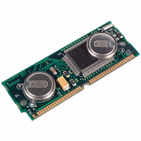
Manufacturer Part Number
DS2250-32-16+
Description
IC MCU 32KB 16MHZ 40-SIMM
Manufacturer
Maxim Integrated Products
Series
DS225xr
Datasheet
1.DS2250-32-16.pdf
(18 pages)
Specifications of DS2250-32-16+
Core Processor
8051
Core Size
8-Bit
Speed
16MHz
Connectivity
SIO, UART/USART
Peripherals
Power-Fail Reset, WDT
Number Of I /o
32
Program Memory Type
SRAM
Ram Size
32K x 8
Voltage - Supply (vcc/vdd)
4.75 V ~ 5.25 V
Oscillator Type
External
Operating Temperature
0°C ~ 70°C
Package / Case
40-SIMM
Processor Series
DS2250
Core
8051
Data Bus Width
8 bit
Program Memory Size
32 KB
Data Ram Size
32 KB
Interface Type
3-Wire, RS-232, UART
Maximum Clock Frequency
16 MHz
Number Of Programmable I/os
32
Number Of Timers
2
Operating Supply Voltage
4.75 V to 5.25 V
Maximum Operating Temperature
+ 70 C
Mounting Style
SMD/SMT
Minimum Operating Temperature
0 C
Lead Free Status / RoHS Status
Lead free / RoHS Compliant
Eeprom Size
-
Program Memory Size
-
Data Converters
-
Lead Free Status / Rohs Status
Details


PIN DESCRIPTION
26, 28, 30, 32,
4, 6, 8, 10, 12,
34, 36, 38, 40
1, 3, 5, 7, 9,
11, 13, 15
14, 16, 18
35, 37
PIN
17
19
21
23
25
27
29
31
33
39
24
22
20
2
P1.0 - P1.7. General purpose I/O Port 1
RST - Active high reset input. A logic 1 applied to this pin will activate a reset state.
This pin is pulled down internally so this pin can be left unconnected if not used. An
RC power-on reset circuit is not needed and is not recommended.
P3.0 RXD. General purpose I/O port pin 3.0. Also serves as the receive signal for the
on board UART. This pin should not be connected directly to a PC COM port.
P3.1 TXD. General purpose I/O port pin 3.1. Also serves as the transmit signal for the
on board UART. This pin should not be connected directly to a PC COM port.
P3.2
Interrupt 0.
P3.3
Interrupt 1.
P3.4 T0. General purpose I/O port pin 3.4. Also serves as the Timer 0 input.
P3.5 T1. General purpose I/O port pin 3.5. Also serves as the Timer 1 input.
P3.6
bus operation.
P3.7
bus operation.
XTAL2, XTAL1. Used to connect an external crystal to the internal oscillator.
XTAL1 is the input to an inverting amplifier and XTAL2 is the output.
GND - Logic ground.
P2.7-P2.0. General purpose I/O Port 2. Also serves as the MSB of the Expanded
Address bus.
program memory when using the Expanded bus. It is normally an output and should
be unconnected if not used.
time,
DS2250(T) is already in a reset state. The device that pulls down should be open-drain
since it must not interfere with
ALE - Address Latch Enable. Used to de-multiplex the multiplexed Expanded
Address/Data bus on Port 0. This pin is normally connected to the clock input on a
’373 type transparent latch. When using a parallel programmer, this pin also assumes
the
internal memory (or clock) will be available when this pin is at a logic low. Since this
pin is pulled down internally, it should be connected to +5V to use NV RAM. In a
parallel programmer, this pin also serves as V
P0.0-P0.7. General purpose I/O Port 0. This port is open-drain and can not drive a
logic 1. It requires external pullups. Port 0 is also the multiplexed Expanded
Address/Data bus. When used in this mode, it does not require pullups.
V
PSEN
EA
CC
PROG
- External Access. This pin forces the DS2250(T) to behave like an 8031. No
+ - 5 volts.
INT0
INT1
WR
RD
PSEN
- Program Store Enable. This active low signal is used to enable an external
. General purpose I/O port pin. Also serves as the read strobe for Expanded
. General purpose I/O port pin. Also serves as the write strobe for Expanded
. General purpose I/O port pin 3.3. Also serves as the active low External
function for programming pulses.
. General purpose I/O port pin 3.2. Also serves as the active low External
will be pulled down externally. This should only be done once the
PSEN
PSEN
3 of 18
also is used to invoke the Bootstrap Loader. At this
DESCRIPTION
under normal operation.
PP
for super voltage pulses.
Related parts for DS2250-32-16+
Image
Part Number
Description
Manufacturer
Datasheet
Request
R

Part Number:
Description:
IC MCU 64KB 16MHZ 40-SIMM
Manufacturer:
Maxim Integrated Products
Datasheet:
Part Number:
Description:
IC MICROCNTRLR 32X8 16MHZ 40SIMM
Manufacturer:
Maxim Integrated Products
Datasheet:
Part Number:
Description:
IC MICROCNTRLR 64X8 16MHZ 40SIMM
Manufacturer:
Maxim Integrated Products
Datasheet:
Part Number:
Description:
IC MCU 64KB 16MHZ 40-SIMM
Manufacturer:
Maxim Integrated Products
Datasheet:

Part Number:
Description:
Microcontrollers (MCU)
Manufacturer:
Maxim Integrated Products
Part Number:
Description:
MAX7528KCWPMaxim Integrated Products [CMOS Dual 8-Bit Buffered Multiplying DACs]
Manufacturer:
Maxim Integrated Products
Datasheet:
Part Number:
Description:
Single +5V, fully integrated, 1.25Gbps laser diode driver.
Manufacturer:
Maxim Integrated Products
Datasheet:
Part Number:
Description:
Single +5V, fully integrated, 155Mbps laser diode driver.
Manufacturer:
Maxim Integrated Products
Datasheet:
Part Number:
Description:
VRD11/VRD10, K8 Rev F 2/3/4-Phase PWM Controllers with Integrated Dual MOSFET Drivers
Manufacturer:
Maxim Integrated Products
Datasheet:
Part Number:
Description:
Highly Integrated Level 2 SMBus Battery Chargers
Manufacturer:
Maxim Integrated Products
Datasheet:
Part Number:
Description:
Current Monitor and Accumulator with Integrated Sense Resistor; ; Temperature Range: -40°C to +85°C
Manufacturer:
Maxim Integrated Products
Part Number:
Description:
TSSOP 14/A�/RS-485 Transceivers with Integrated 100O/120O Termination Resis
Manufacturer:
Maxim Integrated Products
Part Number:
Description:
TSSOP 14/A�/RS-485 Transceivers with Integrated 100O/120O Termination Resis
Manufacturer:
Maxim Integrated Products
Part Number:
Description:
QFN 16/A�/AC-DC and DC-DC Peak-Current-Mode Converters with Integrated Step
Manufacturer:
Maxim Integrated Products
Part Number:
Description:
TDFN/A/65V, 1A, 600KHZ, SYNCHRONOUS STEP-DOWN REGULATOR WITH INTEGRATED SWI
Manufacturer:
Maxim Integrated Products