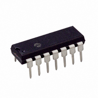
PIC16F684-E/P Microchip Technology, PIC16F684-E/P Datasheet - Page 79

PIC16F684-E/P
Manufacturer Part Number
PIC16F684-E/P
Description
IC PIC MCU FLASH 2KX14 14DIP
Manufacturer
Microchip Technology
Series
PIC® 16Fr
Datasheets
1.PIC16F616T-ISL.pdf
(8 pages)
2.PIC16F688T-ISL.pdf
(688 pages)
3.PIC16F684-ISL.pdf
(4 pages)
4.PIC16F684-ISL.pdf
(192 pages)
5.PIC16F684-ISL.pdf
(6 pages)
6.PIC16F684-IST.pdf
(164 pages)
Specifications of PIC16F684-E/P
Program Memory Type
FLASH
Program Memory Size
3.5KB (2K x 14)
Package / Case
14-DIP (0.300", 7.62mm)
Core Processor
PIC
Core Size
8-Bit
Speed
20MHz
Peripherals
Brown-out Detect/Reset, POR, PWM, WDT
Number Of I /o
12
Eeprom Size
256 x 8
Ram Size
128 x 8
Voltage - Supply (vcc/vdd)
2 V ~ 5.5 V
Data Converters
A/D 8x10b
Oscillator Type
Internal
Operating Temperature
-40°C ~ 125°C
Processor Series
PIC16F
Core
PIC
Data Bus Width
8 bit
Data Ram Size
128 B
Maximum Clock Frequency
20 MHz
Number Of Programmable I/os
12
Number Of Timers
3
Operating Supply Voltage
2 V to 5.5 V
Maximum Operating Temperature
+ 125 C
Mounting Style
Through Hole
3rd Party Development Tools
52715-96, 52716-328, 52717-734
Development Tools By Supplier
PG164130, DV164035, DV244005, DV164005, PG164120, ICE2000, DM163014, DM164120-4
Minimum Operating Temperature
- 40 C
On-chip Adc
8-ch x 10-bit
Lead Free Status / RoHS Status
Lead free / RoHS Compliant
For Use With
DM163029 - BOARD PICDEM FOR MECHATRONICSACICE0207 - MPLABICE 14P 300 MIL ADAPTER
Connectivity
-
Lead Free Status / Rohs Status
Lead free / RoHS Compliant
- PIC16F616T-ISL PDF datasheet
- PIC16F688T-ISL PDF datasheet #2
- PIC16F684-ISL PDF datasheet #3
- PIC16F684-ISL PDF datasheet #4
- PIC16F684-ISL PDF datasheet #5
- PIC16F684-IST PDF datasheet #6
- Current page: 79 of 688
- Download datasheet (3Mb)
Table 4-1:
V
V
V
VLCDADJ
V
V
V
VREG
V
V
WR
Legend: TTL = TTL-compatible input
1997 Microchip Technology Inc.
LCD
LCD
LCD
REF
REF
REF
SS
DD
Pin Name
1
2
3
+
-
ST = Schmitt Trigger input with CMOS levels
SM = SMBus compatible input. An external resistor is required if this pin is used as an output
NPU = N-channel pull-up
No-P diode = No P-diode to V
I = input
P = Power
I/O Descriptions (Cont.’d)
Type
Pin
O
P
P
P
P
P
I
I
I
I
I
Analog
Analog
Analog
Analog
Buffer
Type
TTL
—
—
—
—
—
—
DD
Description
LCD Voltage
LCD Voltage
LCD Voltage
LCD Voltage Generation
Analog High Voltage Reference input.
DR reference voltage output on devices with comparators.
Analog High Voltage Reference input.
Usually multiplexed onto an analog pin.
Analog Low Voltage Reference input.
Usually multiplexed onto an analog pin.
This pin is an output to control the gate of an external N-FET
for voltage regulation.
Ground reference for logic and I/O pins.
Positive supply for logic and I/O pins.
Write control for parallel slave port (See CS and RD pins also).
Section 4. Architecture
CMOS = CMOS compatible input or output
PU = Weak internal pull-up
AN = Analog input or output
O = output
L = LCD Driver
DS31004A-page 4-11
4
Related parts for PIC16F684-E/P
Image
Part Number
Description
Manufacturer
Datasheet
Request
R

Part Number:
Description:
3.5KB Flash, 128B RAM, 18 I/O, CLC, CWG, DDS, 10-bit ADC 20 QFN 4x4mm TUBE
Manufacturer:
Microchip Technology
Datasheet:

Part Number:
Description:
3.5KB Flash, 128B RAM, 18 I/O, CLC, CWG, DDS, 10-bit ADC 20 PDIP .300in TUBE
Manufacturer:
Microchip Technology
Datasheet:

Part Number:
Description:
3.5KB Flash, 128B RAM, 18 I/O, CLC, CWG, DDS, 10-bit ADC 20 SOIC .300in TUBE
Manufacturer:
Microchip Technology
Datasheet:

Part Number:
Description:
3.5KB Flash, 128B RAM, 18 I/O, CLC, CWG, DDS, 10-bit ADC 20 SSOP .209in TUBE
Manufacturer:
Microchip Technology
Datasheet:

Part Number:
Description:
3.5KB Flash, 128B RAM, 18 I/O, CLC, CWG, DDS, 10-bit ADC 20 QFN 4x4mm TUBE
Manufacturer:
Microchip Technology
Datasheet:

Part Number:
Description:
3.5KB Flash, 128B RAM, 18 I/O, CLC, CWG, DDS, 10-bit ADC 20 PDIP .300in TUBE
Manufacturer:
Microchip Technology
Datasheet:

Part Number:
Description:
3.5KB Flash, 128B RAM, 18 I/O, CLC, CWG, DDS, 10-bit ADC 20 SOIC .300in TUBE
Manufacturer:
Microchip Technology
Datasheet:

Part Number:
Description:
3.5KB Flash, 128B RAM, 18 I/O, CLC, CWG, DDS, 10-bit ADC 20 SSOP .209in TUBE
Manufacturer:
Microchip Technology
Datasheet:

Part Number:
Description:
3.5KB Flash, 128B RAM, 18 I/O, CLC, CWG, DDS, 10-bit ADC 20 QFN 4x4mm T/R
Manufacturer:
Microchip Technology
Datasheet:

Part Number:
Description:
3.5KB Flash, 128B RAM, 18 I/O, CLC, CWG, DDS, 10-bit ADC 20 SOIC .300in T/R
Manufacturer:
Microchip Technology
Datasheet:

Part Number:
Description:
3.5KB Flash, 128B RAM, 18 I/O, CLC, CWG, DDS, 10-bit ADC 20 SSOP .209in T/R
Manufacturer:
Microchip Technology
Datasheet:

Part Number:
Description:
3.5KB Flash, 128B RAM, 18 I/O, CLC, CWG, DDS, 10-bit ADC 20 QFN 4x4mm TUBE
Manufacturer:
Microchip Technology
Datasheet:

Part Number:
Description:
3.5KB Flash, 128B RAM, 18 I/O, CLC, CWG, DDS, 10-bit ADC 20 PDIP .300in TUBE
Manufacturer:
Microchip Technology
Datasheet:

Part Number:
Description:
3.5KB Flash, 128B RAM, 18 I/O, CLC, CWG, DDS, 10-bit ADC 20 SOIC .300in TUBE
Manufacturer:
Microchip Technology
Datasheet:

Part Number:
Description:
3.5KB Flash, 128B RAM, 18 I/O, CLC, CWG, DDS, 10-bit ADC 20 SSOP .209in TUBE
Manufacturer:
Microchip Technology
Datasheet:


