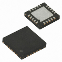
ATTINY84-20MUR Atmel, ATTINY84-20MUR Datasheet - Page 167

ATTINY84-20MUR
Manufacturer Part Number
ATTINY84-20MUR
Description
MCU AVR 8KB FLASH 20MHZ 20QFN
Manufacturer
Atmel
Series
AVR® ATtinyr
Specifications of ATTINY84-20MUR
Core Processor
AVR
Core Size
8-Bit
Speed
20MHz
Connectivity
USI
Peripherals
Brown-out Detect/Reset, POR, PWM, Temp Sensor, WDT
Number Of I /o
12
Program Memory Size
8KB (4K x 16)
Program Memory Type
FLASH
Eeprom Size
512 x 8
Ram Size
512 x 8
Voltage - Supply (vcc/vdd)
2.7 V ~ 5.5 V
Data Converters
A/D 8x10b
Oscillator Type
Internal
Operating Temperature
-40°C ~ 85°C
Package / Case
*
Lead Free Status / RoHS Status
Lead free / RoHS Compliant
- Current page: 167 of 238
- Download datasheet (5Mb)
19.6
8006K–AVR–10/10
High-voltage Serial Programming
If the LSB in RDY/BSY data byte out is ‘1’, a programming operation is still pending. Wait until
this bit returns ‘0’ before the next instruction is carried out.
Within the same page, the low data byte must be loaded prior to the high data byte.
After data is loaded to the page buffer, program the EEPROM page, see
166.
This section describes how to program and verify Flash Program memory, EEPROM Data mem-
ory, Lock bits and Fuse bits in the ATtiny24/44/84.
Figure 19-3. High-voltage Serial Programming
Table 19-13. Pin Name Mapping
The minimum period for the Serial Clock Input (SCI) during High-voltage Serial Programming is
220 ns.
Table 19-14. Pin Values Used to Enter Programming Mode
Signal Name in High-voltage
Serial Programming Mode
SDI
SII
SDO
SCI
Pin
PA0
PA1
PA2
SCI
+11.5 - 12.5V
Symbol
Prog_enable[0]
Prog_enable[1]
Prog_enable[2]
PB3
PB0
PA2:0
GND
PA5
Pin Name
PA6
PA4
PB0
(RESET)
I/O
O
I
I
I
VCC
PA4
PA5
PA6
Function
Serial Data Input
Serial Instruction Input
Serial Data Output
Serial Clock Input (min. 220ns period)
+4.5 - 5.5V
ATtiny24/44/84
SDO
SII
SDI
Figure 19-2 on page
Value
0
0
0
167
Related parts for ATTINY84-20MUR
Image
Part Number
Description
Manufacturer
Datasheet
Request
R

Part Number:
Description:
Manufacturer:
Atmel Corporation
Datasheet:

Part Number:
Description:
Manufacturer:
Atmel Corporation
Datasheet:

Part Number:
Description:
IC MCU AVR 8K FLASH 20MHZ 20-QFN
Manufacturer:
Atmel
Datasheet:

Part Number:
Description:
MCU AVR 8K ISP FLASH 2.7V 14SOIC
Manufacturer:
Atmel
Datasheet:

Part Number:
Description:
MCU AVR 8K FLASH 15MHZ 20-QFN
Manufacturer:
Atmel
Datasheet:

Part Number:
Description:
IC MCU AVR 8K FLASH 20MHZ 14-DIP
Manufacturer:
Atmel
Datasheet:

Part Number:
Description:
MCU AVR 8KB FLASH 10MHZ 14SOIC
Manufacturer:
Atmel
Datasheet:

Part Number:
Description:
IC, MCU, 8BIT, 2K FLASH, 20SOIC
Manufacturer:
Atmel
Datasheet:

Part Number:
Description:
IC, MCU, 8BIT, 2K FLASH, 20PDIP
Manufacturer:
Atmel
Datasheet:

Part Number:
Description:
IC, MCU, 8BIT, 8K FLASH, 20PDIP
Manufacturer:
Atmel
Datasheet:

Part Number:
Description:
IC, MCU, 8BIT, 8K FLASH, 20SOIC
Manufacturer:
Atmel
Datasheet:

Part Number:
Description:
DEV KIT FOR AVR/AVR32
Manufacturer:
Atmel
Datasheet:

Part Number:
Description:
INTERVAL AND WIPE/WASH WIPER CONTROL IC WITH DELAY
Manufacturer:
ATMEL Corporation
Datasheet:

Part Number:
Description:
Low-Voltage Voice-Switched IC for Hands-Free Operation
Manufacturer:
ATMEL Corporation
Datasheet:


