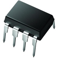
PIC12LCE673-04I/P Microchip Technology, PIC12LCE673-04I/P Datasheet - Page 5

PIC12LCE673-04I/P
Manufacturer Part Number
PIC12LCE673-04I/P
Description
IC MCU OTP 1KX14 LV A/D EE 8DIP
Manufacturer
Microchip Technology
Series
PIC® 12Cr
Specifications of PIC12LCE673-04I/P
Core Processor
PIC
Core Size
8-Bit
Speed
4MHz
Peripherals
POR, WDT
Number Of I /o
5
Program Memory Size
1.75KB (1K x 14)
Program Memory Type
OTP
Eeprom Size
16 x 8
Ram Size
128 x 8
Voltage - Supply (vcc/vdd)
2.5 V ~ 5.5 V
Data Converters
A/D 4x8b
Oscillator Type
Internal
Operating Temperature
-40°C ~ 85°C
Package / Case
8-DIP (0.300", 7.62mm)
Processor Series
PIC12LC
Core
PIC
Data Bus Width
8 bit
Data Ram Size
128 B
Maximum Clock Frequency
4 MHz
Number Of Programmable I/os
5
Number Of Timers
8
Operating Supply Voltage
2.5 V to 5.5 V
Maximum Operating Temperature
+ 85 C
Mounting Style
Through Hole
3rd Party Development Tools
52715-96, 52716-328, 52717-734
Development Tools By Supplier
ICE2000
Minimum Operating Temperature
- 40 C
On-chip Adc
8
Data Rom Size
128 B
Height
3.3 mm
Length
9.27 mm
Supply Voltage (max)
5.5 V
Supply Voltage (min)
2.5 V
Width
6.35 mm
Lead Free Status / RoHS Status
Lead free / RoHS Compliant
Connectivity
-
Lead Free Status / Rohs Status
Details
Available stocks
Company
Part Number
Manufacturer
Quantity
Price
Part Number:
PIC12LCE673-04I/P
Manufacturer:
MICROCHIP/微芯
Quantity:
20 000
2.
Correction for the “OSCCAL” Register, Section 4.2.2.7,
is shown.
REGISTER 4-7:
3.
Clarification to the “GPIO”, Section 5.1 is provided.
New I/O drawings were added.
2001 Microchip Technology Inc.
Module:
4.2.2.7
The Oscillator Calibration (OSCCAL) Register is
used to calibrate the internal 4 MHz oscillator. It
contains six bits for calibration. Increasing the
value increases the frequency.
Module:
5.1
GPIO is an 8-bit I/O register. Only the low order 6
bits are used (GP<5:0>). Bits 6 and 7 (SDA and
SCL, respectively) are used by the EEPROM
peripheral on the PIC12CE673/674. Refer to Sec-
tion 6.0 and Appendix B for use of SDA and SCL.
Please note that GP3 is an input only pin. The con-
figuration word can set several
functions. When acting as alternate functions, the
pins will read as ‘0’ during port read.
Pins GP0, GP1 and GP3 can be configured with
weak pull-ups and also with interrupt-on-change.
The interrupt on change and weak pull-up func-
tions are not pin selectable. If pin 4, (GP3), is con-
figured as MCLR, a weak pull-up is always on.
Interrupt-on-change for this pin is not set and GP3
will read as '0'. Interrupt-on-change is enabled by
setting bit GPIE, INTCON<3>.
The interrupt can wake the device from SLEEP.
The user, in the interrupt service routine, can clear
the interrupt in the following manner:
a)
match condition.
b)
A mismatch condition will continue to set flag bit
GPIF. Reading GPIO will end the mismatch condi-
tion and allow flag bit GPIF to be cleared.
Note that external oscillator use overrides the
GPIO functions on GP4 and GP5.
Any read or write of GPIO will end the mis-
Clear flag bit GPIF.
bit 7-2
bit 1-0
GPIO
OSCCAL REGISTER
OSCCAL Register
GPIO Register
OSCCAL REGISTER (ADDRESS 8Fh)
CAL<5:0>: Calibration
Unimplemented: Read as ’0’
bit 7
Legend:
R = Readable bit
- n = Value at POR
R/W-1
CAL5
R/W-0
CAL4
I/O’s to alternate
R/W-0
CAL3
W = Writable bit
’1’ = Bit is set
R/W-0
CAL2
FIGURE 5-1:
Interrupt-on-Change
Data bus
PORT
PORT
TRIS
TRIS
WR
WR
RD
RD
D
D
U = Unimplemented bit, read as ‘0’
’0’ = Bit is cleared
To A/D Converter
CK
CK
R/W-0
CAL1
GPPU
Q
Q
Q
Q
GP0 and GP1 Block Diagram
RD PORT
R/W-0
CAL0
PIC12C67X
Analog
Mode
Q
Q
Input
x = Bit is unknown
EN
EN
D
D
U-0
—
DS80067C-page 5
V
Weak
DD
V
V
DD
SS
U-0
—
I/O Pin
bit 0


