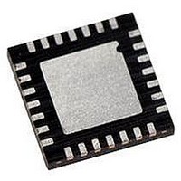
PIC18LF27J53-I/ML Microchip Technology, PIC18LF27J53-I/ML Datasheet - Page 17

PIC18LF27J53-I/ML
Manufacturer Part Number
PIC18LF27J53-I/ML
Description
IC PIC MCU 128KB FLASH 28QFN
Manufacturer
Microchip Technology
Series
PIC® XLP™ 18Fr
Datasheets
1.PIC18LF24J10-ISS.pdf
(32 pages)
2.PIC18F26J13-ISS.pdf
(496 pages)
3.PIC18F26J53-ISS.pdf
(586 pages)
4.PIC18F26J53-ISS.pdf
(12 pages)
Specifications of PIC18LF27J53-I/ML
Core Size
8-Bit
Program Memory Size
128KB (64K x 16)
Core Processor
PIC
Speed
48MHz
Connectivity
I²C, LIN, SPI, UART/USART, USB
Peripherals
Brown-out Detect/Reset, POR, PWM, WDT
Number Of I /o
22
Program Memory Type
FLASH
Ram Size
3.8K x 8
Voltage - Supply (vcc/vdd)
2 V ~ 2.75 V
Data Converters
A/D 10x10b/12b
Oscillator Type
Internal
Operating Temperature
-40°C ~ 85°C
Package / Case
*
Controller Family/series
PIC18
Cpu Speed
48MHz
Digital Ic Case Style
QFN
Supply Voltage Range
1.8V To 3.6V
Embedded Interface Type
I2C, SPI, USART
Rohs Compliant
Yes
Lead Free Status / RoHS Status
Lead free / RoHS Compliant
Eeprom Size
-
Lead Free Status / RoHS Status
Lead free / RoHS Compliant, Lead free / RoHS Compliant
Available stocks
Company
Part Number
Manufacturer
Quantity
Price
Company:
Part Number:
PIC18LF27J53-I/ML
Manufacturer:
ATMEL
Quantity:
101
4.2
The verify step involves reading back the code memory
space and comparing it against the copy held in the
programmer’s buffer. Because the Flash Configuration
Words are stored at the end of program memory, it is
verified with the rest of the code at this time.
The verify process is shown in the flowchart in
Figure 4-2. Memory reads occur a single byte at a time,
so two bytes must be read to compare against the word
in the programmer’s buffer. Refer to Section 4.1
“Read Code Memory” for implementation details of
reading code memory.
FIGURE 4-2:
© 2009 Microchip Technology Inc.
Note:
Verify Code Memory and
Configuration Word
No
Because the Flash Configuration Word
contains the device code protection bit,
code memory should be verified immedi-
ately after writing if code protection is
enabled. This is because the device will not
be readable or verifiable if a device Reset
occurs after the Flash Configuration Words
(and the CP0 bit) have been cleared.
with Post-Increment
with Post-Increment
Set TBLPTR = 0
Read High Byte
Read Low Byte
Word = Expect
Code Memory
Verified?
Data?
Does
Done
Start
VERIFY CODE
MEMORY FLOW
All
Yes
Yes
No
PIC18F2XJXX/4XJXX FAMILY
Failure,
Report
Error
4.3
The term “Blank Check” means to verify that the device
has no programmed memory cells. All memories must
be verified: code memory and Configuration bits. The
Device ID registers (3FFFFEh:3FFFFFh) should be
ignored.
A “blank” or “erased” memory cell will read as a ‘1’, so
Blank Checking a device merely means to verify that all
bytes read as FFh. The overall process flow is shown
in Figure 4-3.
Given that Blank Checking is merely code verification
with FFh expect data, refer to Section 4.2 “Verify Code
Memory and Configuration Word” for implementation
details.
FIGURE 4-3:
Blank Check Device
Blank Check
Device
Blank?
Abort
Start
Is
No
BLANK CHECK FLOW
Yes
Continue
DS39687E-page 17


