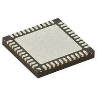
PIC18LF47J53-I/ML Microchip Technology, PIC18LF47J53-I/ML Datasheet - Page 19

PIC18LF47J53-I/ML
Manufacturer Part Number
PIC18LF47J53-I/ML
Description
IC PIC MCU 128KB FLASH 44QFN
Manufacturer
Microchip Technology
Series
PIC® XLP™ 18Fr
Datasheets
1.PIC18LF24J10-ISS.pdf
(32 pages)
2.PIC18F26J13-ISS.pdf
(496 pages)
3.PIC18F26J53-ISS.pdf
(586 pages)
4.PIC18F26J53-ISS.pdf
(12 pages)
Specifications of PIC18LF47J53-I/ML
Core Size
8-Bit
Program Memory Size
128KB (64K x 16)
Core Processor
PIC
Speed
48MHz
Connectivity
I²C, LIN, SPI, UART/USART, USB
Peripherals
Brown-out Detect/Reset, POR, PWM, WDT
Number Of I /o
34
Program Memory Type
FLASH
Ram Size
3.8K x 8
Voltage - Supply (vcc/vdd)
2 V ~ 2.75 V
Data Converters
A/D 13x10b/12b
Oscillator Type
Internal
Operating Temperature
-40°C ~ 85°C
Package / Case
*
Controller Family/series
PIC18
Cpu Speed
48MHz
Digital Ic Case Style
QFN
Supply Voltage Range
1.8V To 3.6V
Embedded Interface Type
I2C, SPI, USART
Rohs Compliant
Yes
Lead Free Status / RoHS Status
Lead free / RoHS Compliant
Eeprom Size
-
Lead Free Status / RoHS Status
Lead free / RoHS Compliant, Lead free / RoHS Compliant
TABLE 5-3:
© 2009 Microchip Technology Inc.
DEBUG
XINST
STVREN
WDTEN
CP0
IESO
FCMEN
FOSC2
FOSC<1:0>
WDTPS<3:0>
CCP2MX
Bit Name
PIC18F45J10 FAMILY DEVICES: BIT DESCRIPTIONS
Configuration
CONFIG1H
CONFIG2H
CONFIG3H
CONFIG1L
CONFIG1L
CONFIG1L
CONFIG1L
CONFIG2L
CONFIG2L
CONFIG2L
CONFIG2L
Words
Background Debugger Enable bit
1 = Background debugger disabled, RB6 and RB7 configured as general
0 = Background debugger enabled, RB6 and RB7 are dedicated to in-circuit debug
Extended Instruction Set Enable bit
1 = Instruction set extension and Indexed Addressing mode enabled
0 = Instruction set extension and Indexed Addressing mode disabled
Stack Overflow/Underflow Reset Enable bit
1 = Reset on stack overflow/underflow enabled
0 = Reset on stack overflow/underflow disabled
Watchdog Timer Enable bit
1 = WDT enabled
0 = WDT disabled (control is placed on SWDTEN bit)
Code Protection bit
1 = Program memory is not code-protected
0 = Program memory is code-protected
Internal/External Oscillator Switchover bit
1 = Oscillator Switchover mode enabled
0 = Oscillator Switchover mode disabled
Fail-Safe Clock Monitor Enable bit
1 = Fail-Safe Clock Monitor enabled
0 = Fail-Safe Clock Monitor disabled
Default Oscillator Select bit
1 = Clock designated by FOSC<1:0> is enabled as system clock when
0 = INTRC is enabled as system clock when OSCCON<1:0> = 00
Primary Oscillator Select bits
11 = EC oscillator, PLL enabled and under software control, CLKO function on OSC2
10 = EC oscillator, CLKO function on OSC2
01 = HS oscillator, PLL enabled and under software control
00 = HS oscillator
Watchdog Timer Postscale Select bits
1111 = 1:32,768
1110 = 1:16,384
1101 = 1:8,192
1100 = 1:4,096
1011 = 1:2,048
1010 = 1:1,024
1001 = 1:512
1000 = 1:256
0111 = 1:128
0110 = 1:64
0101 = 1:32
0100 = 1:16
0011 = 1:8
0010 = 1:4
0001 = 1:2
0000 = 1:1
CCP2 MUX bit
1 = CCP2 is multiplexed with RC1
0 = CCP2 is multiplexed with RB3
PIC18F2XJXX/4XJXX FAMILY
purpose I/O pins
(Legacy mode)
OSCCON<1:0> = 00
Description
DS39687E-page 19


