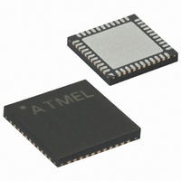
ATMEGA644V-10MU Atmel, ATMEGA644V-10MU Datasheet - Page 288

ATMEGA644V-10MU
Manufacturer Part Number
ATMEGA644V-10MU
Description
IC AVR MCU FLASH 64K 44-QFN
Manufacturer
Atmel
Series
AVR® ATmegar
Specifications of ATMEGA644V-10MU
Core Processor
AVR
Core Size
8-Bit
Speed
10MHz
Connectivity
I²C, SPI, UART/USART
Peripherals
Brown-out Detect/Reset, POR, PWM, WDT
Number Of I /o
32
Program Memory Size
64KB (32K x 16)
Program Memory Type
FLASH
Eeprom Size
2K x 8
Ram Size
4K x 8
Voltage - Supply (vcc/vdd)
1.8 V ~ 5.5 V
Data Converters
A/D 8x10b
Oscillator Type
Internal
Operating Temperature
-40°C ~ 85°C
Package / Case
44-VQFN Exposed Pad
Package
44QFN EP
Device Core
AVR
Family Name
ATmega
Maximum Speed
10 MHz
Operating Supply Voltage
2.5|3.3|5 V
Data Bus Width
8 Bit
Number Of Programmable I/os
32
Interface Type
JTAG/SPI/TWI/USART
On-chip Adc
8-chx10-bit
Number Of Timers
3
Processor Series
ATMEGA64x
Core
AVR8
Data Ram Size
4 KB
Maximum Clock Frequency
20 MHz
Maximum Operating Temperature
+ 85 C
Mounting Style
SMD/SMT
Minimum Operating Temperature
- 40 C
For Use With
ATSTK600-TQFP44 - STK600 SOCKET/ADAPTER 44-TQFPATSTK600 - DEV KIT FOR AVR/AVR32770-1007 - ISP 4PORT ATMEL AVR MCU SPI/JTAGATAVRISP2 - PROGRAMMER AVR IN SYSTEM
Lead Free Status / RoHS Status
Lead free / RoHS Compliant
Available stocks
Company
Part Number
Manufacturer
Quantity
Price
Part Number:
ATMEGA644V-10MU
Manufacturer:
ATMEL/爱特梅尔
Quantity:
20 000
- Current page: 288 of 376
- Download datasheet (8Mb)
288
ATmega644
The XA1/XA0 pins determine the action executed when the XTAL1 pin is given a positive pulse.
The bit coding is shown in
When pulsing WR or OE, the command loaded determines the action executed. The different
commands are shown in
Figure 25-1. Parallel Programming
Note:
Table 25-9.
Programming Mode
Signal Name in
RDY/BSY
1. Unused Pins should be left floating.
PAGEL
DATA
BS1
XA0
XA1
BS2
WR
OE
Pin Name Mapping
Table
RDY/BSY
Pin Name
Table
PAGEL
PB7-0
+12V
BS2
PD1
PD2
PD3
PD4
PD5
PD6
PD7
BS1
XA0
XA1
PA0
WR
OE
25-13.
25-12.
(1)
I/O
I/O
PD1
PD2
PD3
PD4
PD5
PD6
PD7
RESET
XTAL1
GND
O
PA0
I
I
I
I
I
I
I
Function
0: Device is busy programming, 1: Device is ready for
new command.
Output Enable (Active low).
Write Pulse (Active low).
XTAL Action Bit 0
XTAL Action Bit 1
Program Memory and EEPROM data Page Load.
Byte Select 2.
Byte Select 1.
Bi-directional Data bus (Output when OE is low).
PB7 - PB0
AVCC
VCC
+5V
+5V
DATA
2593N–AVR–07/10
Related parts for ATMEGA644V-10MU
Image
Part Number
Description
Manufacturer
Datasheet
Request
R

Part Number:
Description:
Manufacturer:
Atmel Corporation
Datasheet:

Part Number:
Description:
IC AVR MCU FLASH 64K 44-QFN
Manufacturer:
Atmel
Datasheet:

Part Number:
Description:
IC AVR MCU FLASH 64K 44TQFP
Manufacturer:
Atmel
Datasheet:

Part Number:
Description:
IC AVR MCU FLASH 64K 40DIP
Manufacturer:
Atmel
Datasheet:

Part Number:
Description:
MCU AVR 64K FLASH 20MHZ 44TQFP
Manufacturer:
Atmel
Datasheet:

Part Number:
Description:
MCU AVR 64K FLASH 20MHZ 44QFN
Manufacturer:
Atmel
Datasheet:

Part Number:
Description:
Atmega644 8-bit Avr Microcontroller With 64k Bytes In-system Programmable Flash
Manufacturer:
ATMEL Corporation
Datasheet:

Part Number:
Description:
Manufacturer:
Atmel Corporation
Datasheet:

Part Number:
Description:
Manufacturer:
ATMEL Corporation
Datasheet:

Part Number:
Description:
Manufacturer:
ATMEL Corporation
Datasheet:

Part Number:
Description:
IC AVR MCU 64K 16MHZ 5V 64TQFP
Manufacturer:
Atmel
Datasheet:

Part Number:
Description:
IC AVR MCU 64K 16MHZ 5V 64-QFN
Manufacturer:
Atmel
Datasheet:


