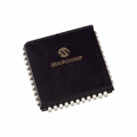
PIC16F877T-20I/L Microchip Technology, PIC16F877T-20I/L Datasheet - Page 226

PIC16F877T-20I/L
Manufacturer Part Number
PIC16F877T-20I/L
Description
IC MCU FLASH 8KX14 EE 44PLCC
Manufacturer
Microchip Technology
Series
PIC® 16Fr
Datasheets
1.PIC16F616T-ISL.pdf
(8 pages)
2.PIC16F688T-ISL.pdf
(688 pages)
3.PIC16C770-ISO.pdf
(8 pages)
4.PIC16F873-04SO.pdf
(218 pages)
5.PIC16F873-04SO.pdf
(5 pages)
6.PIC16F873-04SO.pdf
(5 pages)
Specifications of PIC16F877T-20I/L
Core Processor
PIC
Core Size
8-Bit
Speed
20MHz
Connectivity
I²C, SPI, UART/USART
Peripherals
Brown-out Detect/Reset, POR, PWM, WDT
Number Of I /o
33
Program Memory Size
14KB (8K x 14)
Program Memory Type
FLASH
Eeprom Size
256 x 8
Ram Size
368 x 8
Voltage - Supply (vcc/vdd)
4 V ~ 5.5 V
Data Converters
A/D 8x10b
Oscillator Type
External
Operating Temperature
-40°C ~ 85°C
Package / Case
44-PLCC
For Use With
DVA16XL441 - ADAPTER DEVICE ICE 44PLCC309-1040 - ADAPTER 44-PLCC ZIF TO 40-DIP309-1039 - ADAPTER 44-PLCC TO 40-DIP
Lead Free Status / RoHS Status
Lead free / RoHS Compliant
Available stocks
Company
Part Number
Manufacturer
Quantity
Price
Company:
Part Number:
PIC16F877T-20I/L
Manufacturer:
Microchip Technology
Quantity:
10 000
- PIC16F616T-ISL PDF datasheet
- PIC16F688T-ISL PDF datasheet #2
- PIC16C770-ISO PDF datasheet #3
- PIC16F873-04SO PDF datasheet #4
- PIC16F873-04SO PDF datasheet #5
- PIC16F873-04SO PDF datasheet #6
- Current page: 226 of 688
- Download datasheet (3Mb)
PICmicro MID-RANGE MCU FAMILY
15.3
15.3.1
DS31015A-page 15-6
Operation
SPI Mode
The SPI mode allows 8-bits of data to be synchronously transmitted and received simulta-
neously. All four modes of SPI are supported, as well as Microwire™ (sample edge) when the
SPI is in the master mode.
To accomplish communication, typically three pins are used:
• Serial Data Out (SDO)
• Serial Data In (SDI)
• Serial Clock (SCK)
Additionally a fourth pin may be used when in a slave mode of operation:
• Slave Select (SS)
When initializing the SPI, several options need to be specified. This is done by programming the
appropriate control bits in the SSPCON register (SSPCON<5:0>) and SSPSTAT<7:6>. These
control bits allow the following to be specified:
• Master Mode (SCK is the clock output)
• Slave Mode (SCK is the clock input)
• Clock Polarity (Idle state of SCK)
• Clock edge (output data on rising/falling edge of SCK)
• Data Input Sample Phase
• Clock Rate (Master mode only)
• Slave Select Mode (Slave mode only)
Figure 15-1
Figure 15-1:
shows the block diagram of the SSP module, when in SPI mode.
SSP Block Diagram (SPI Mode)
SDI
SDO
SS
SCK
Read
SS Control
TRIS bit of SCK pin
Select
Edge
Enable
bit0
Select
Edge
SSPBUF reg
SSPM3:SSPM0
SSPSR reg
Clock Select
4
2
shift clock
Write
Prescaler
4, 16, 64
data bus
Internal
TMR2 output
1997 Microchip Technology Inc.
T
CY
2
Related parts for PIC16F877T-20I/L
Image
Part Number
Description
Manufacturer
Datasheet
Request
R

Part Number:
Description:
IC MCU FLASH 8KX14 EE 44-MQFP
Manufacturer:
Microchip Technology
Datasheet:

Part Number:
Description:
IC MCU FLASH 8KX14 EE 44PLCC
Manufacturer:
Microchip Technology
Datasheet:

Part Number:
Description:
IC MCU FLASH 8KX14 EE 44TQFP
Manufacturer:
Microchip Technology
Datasheet:

Part Number:
Description:
IC MCU FLASH 8KX14 EE 44-MQFP
Manufacturer:
Microchip Technology
Datasheet:

Part Number:
Description:
IC MCU FLASH 8KX14 EE 44PLCC
Manufacturer:
Microchip Technology
Datasheet:

Part Number:
Description:
IC MCU FLASH 8KX14 EE 44TQFP
Manufacturer:
Microchip Technology
Datasheet:

Part Number:
Description:
IC MCU FLASH 8KX14 EE 44TQFP
Manufacturer:
Microchip Technology
Datasheet:

Part Number:
Description:
IC MCU FLASH 8KX14 EE 44PLCC
Manufacturer:
Microchip Technology
Datasheet:

Part Number:
Description:
IC MCU FLASH 8KX14 EE 44-MQFP
Manufacturer:
Microchip Technology
Datasheet:

Part Number:
Description:
IC MCU FLASH 8KX14 EE 44TQFP
Manufacturer:
Microchip Technology
Datasheet:

Part Number:
Description:
IC MCU FLASH 8KX14 EE 44PLCC
Manufacturer:
Microchip Technology
Datasheet:

Part Number:
Description:
IC MCU FLASH 8KX14 EE 44PLCC
Manufacturer:
Microchip Technology
Datasheet:

Part Number:
Description:
IC MCU FLASH 8KX14 EE 44-MQFP
Manufacturer:
Microchip Technology
Datasheet:

Part Number:
Description:
IC MCU FLASH 8KX14 EE 44-MQFP
Manufacturer:
Microchip Technology
Datasheet:

Part Number:
Description:
IC MCU FLASH 8KX14 EE 44TQFP
Manufacturer:
Microchip Technology
Datasheet:


