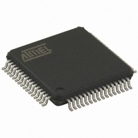
AT32UC3B064-A2UT Atmel, AT32UC3B064-A2UT Datasheet - Page 85

AT32UC3B064-A2UT
Manufacturer Part Number
AT32UC3B064-A2UT
Description
IC MCU AVR32 64KB FLASH 64-TQFP
Manufacturer
Atmel
Series
AVR®32 UC3r
Specifications of AT32UC3B064-A2UT
Core Processor
AVR
Core Size
32-Bit
Speed
60MHz
Connectivity
I²C, IrDA, SPI, SSC, UART/USART, USB
Peripherals
Brown-out Detect/Reset, DMA, POR, PWM, WDT
Number Of I /o
44
Program Memory Size
64KB (64K x 8)
Program Memory Type
FLASH
Ram Size
16K x 8
Voltage - Supply (vcc/vdd)
1.65 V ~ 1.95 V
Data Converters
A/D 8x10b
Oscillator Type
Internal
Operating Temperature
-40°C ~ 85°C
Package / Case
64-TQFP, 64-VQFP
Controller Family/series
AT32UC3B
No. Of I/o's
44
Ram Memory Size
16KB
Cpu Speed
60MHz
No. Of Timers
1
Rohs Compliant
Yes
Processor Series
AT32UC3x
Core
AVR32
Data Bus Width
32 bit
Data Ram Size
16 KB
Interface Type
2-Wire, SPI, USART
Maximum Clock Frequency
60 MHz
Number Of Programmable I/os
44
Number Of Timers
3
Maximum Operating Temperature
+ 85 C
Mounting Style
SMD/SMT
3rd Party Development Tools
EWAVR32, EWAVR32-BL
Development Tools By Supplier
ATAVRDRAGON, ATSTK500, ATSTK600, ATAVRISP2, ATAVRONEKIT, ATEXTWIFI, ATEVK1101
Minimum Operating Temperature
- 40 C
On-chip Adc
10 bit, 8 Channel
For Use With
ATAVRONEKIT - KIT AVR/AVR32 DEBUGGER/PROGRMMR770-1008 - ISP 4PORT ATMEL AVR32 MCU SPIATSTK600-TQFP64-2 - STK600 SOCKET/ADAPTER FOR 64-TQFATEVK1101 - KIT DEV/EVAL FOR AVR32 AT32UC3B
Lead Free Status / RoHS Status
Lead free / RoHS Compliant
Eeprom Size
-
Lead Free Status / Rohs Status
Details
Available stocks
Company
Part Number
Manufacturer
Quantity
Price
32059K–03/2011
- HMATRIX
- FLASHC
3. The RTS output does not function correctly in hardware handshaking mode
4. Corruption after receiving too many bits in SPI slave mode
5. USART slave synchronous mode external clock must be at least 9 times lower in fre-
1. In the HMATRIX PRAS and PRBS registers MxPR fields are only two bits
1. Reading from on-chip flash may fail after a flash fuse write operation (FLASHC LP,
The RTS signal is not generated properly when the USART receives data in hardware hand-
shaking mode. When the Peripheral DMA receive buffer becomes full, the RTS output
should go high, but it will stay low.
Fix/Workaround
Do not use the hardware handshaking mode of the USART. If it is necessary to drive the
RTS output high when the Peripheral DMA receive buffer becomes full, use the normal
mode of the USART. Configure the Peripheral DMA Controller to signal an interrupt when
the receive buffer is full. In the interrupt handler code, write a one to the RTSDIS bit in the
USART Control Register (CR). This will drive the RTS output high. After the next DMA trans-
fer is started and a receive buffer is available, write a one to the RTSEN bit in the USART
CR so that RTS will be driven low.
If the USART is in SPI slave mode and receives too much data bits (ex: 9bitsinstead of 8
bits) by the the SPI master, an error occurs . After that, the next reception may be corrupted
even if the frame is correct and the USART has been disabled, reseted by a soft reset and
re-enabled.
Fix/Workaround
None.
quency than CLK_USART
When the USART is operating in slave synchronous mode with an external clock, the fre-
quency of the signal provided on CLK must be at least 9 times lower than CLK_USART.
Fix/Workaround
When the USART is operating in slave synchronous mode with an external clock, provide a
signal on CLK that has a frequency at least 9 times lower than CLK_USART.
In the HMATRIX PRAS and PRBS registers MxPR fields are only two bits wide, instead of
four bits. The unused bits are undefined when reading the registers.
Fix/Workaround
Mask undefined bits when reading PRAS and PRBS.
UP, WGPB, EGPB, SSB, PGPFB, EAGPF commands).
After a flash fuse write operation (FLASHC LP, UP, WGPB, EGPB, SSB, PGPFB, EAGPF
commands), the following flash read access may return corrupted data. This erratum does
not affect write operations to regular flash memory.
Fix/Workaround
The flash fuse write operation (FLASHC LP, UP, WGPB, EGPB, SSB, PGPFB, EAGPF
commands) must be issued from internal RAM. After the write operation, perform a dummy
flash page write operation (FLASHC WP). Content and location of this page is not important
and filling the write buffer with all one (FFh) will leave the current flash content unchanged. It
is then safe to read and fetch code from the flash.
AT32UC3B
85


