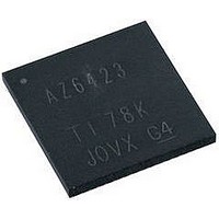
PIC24FJ128DA206-I/MR Microchip Technology, PIC24FJ128DA206-I/MR Datasheet - Page 163

PIC24FJ128DA206-I/MR
Manufacturer Part Number
PIC24FJ128DA206-I/MR
Description
MCU PIC 16BIT FLASH 128K 64VQFN
Manufacturer
Microchip Technology
Series
PIC® 24Fr
Specifications of PIC24FJ128DA206-I/MR
Core Size
16-Bit
Program Memory Size
128KB (43K x 24)
Core Processor
PIC
Speed
32MHz
Connectivity
I²C, IrDA, SPI, UART/USART, USB OTG
Peripherals
Brown-out Detect/Reset, GFX, LVD, POR, PWM, WDT
Number Of I /o
52
Program Memory Type
FLASH
Ram Size
96K x 8
Voltage - Supply (vcc/vdd)
2.2 V ~ 3.6 V
Data Converters
A/D 16x10b
Oscillator Type
Internal
Operating Temperature
-40°C ~ 85°C
Package / Case
64-VFQFN, Exposed Pad
Controller Family/series
PIC24
No. Of I/o's
52
Ram Memory Size
96KB
Cpu Speed
32MHz
No. Of Timers
5
No. Of Pwm Channels
9
Processor Series
PIC24FJ
Core
PIC
Data Bus Width
16 bit
Data Ram Size
96 KB
Interface Type
I2C, SPI, UART
Maximum Clock Frequency
32 MHz
Number Of Programmable I/os
29
Number Of Timers
5
Operating Supply Voltage
2.2 V to 3.6 V
Maximum Operating Temperature
+ 85 C
Mounting Style
SMD/SMT
3rd Party Development Tools
52713-733, 52714-737, 53276-922, EWDSPIC
Development Tools By Supplier
PG164130, DV164035, DV244005, DV164005, AC164127-4, AC164127-6, AC164139, DM240312, DV164039
Minimum Operating Temperature
- 40 C
On-chip Adc
10 bit, 16 Channel
Lead Free Status / RoHS Status
Lead free / RoHS Compliant
Eeprom Size
-
Lead Free Status / Rohs Status
Details
- Current page: 163 of 408
- Download datasheet (4Mb)
10.3
The input change notification function of the I/O ports
allows the PIC24FJ256DA210 family of devices to gen-
erate interrupt requests to the processor in response to
a Change-Of-State (COS) on selected input pins. This
feature is capable of detecting input Change-Of-States,
even in Sleep mode, when the clocks are disabled.
Depending on the device pin count, there are up to
84 external inputs that may be selected (enabled) for
generating an interrupt request on a Change-Of-State.
Registers, CNEN1 through CNEN6, contain the inter-
rupt enable control bits for each of the CN input pins.
Setting any of these bits enables a CN interrupt for the
corresponding pins.
Each CN pin has a both a weak pull-up and a weak
pull-down connected to it. The pull-ups act as a current
source that is connected to the pin, while the
pull-downs act as a current sink that is connected to the
pin. These eliminate the need for external resistors
EXAMPLE 10-1:
EXAMPLE 10-2:
2010 Microchip Technology Inc.
MOV
MOV
NOP
BTSS
TRISB = 0xFF00;
Nop();
If (PORTBbits.RB13){ };
Input Change Notification
0xFF00, W0
W0, TRISB
PORTB, #13
PORT WRITE/READ IN ASSEMBLY
PORT WRITE/READ IN ‘C’
; Configure PORTB<15:8> as inputs
; and PORTB<7:0> as outputs
; Next Instruction
; Delay 1 cycle
// Configure PORTB<15:8> as inputs and PORTB<7:0> as outputs
// Delay 1 cycle
// Next Instruction
PIC24FJ256DA210 FAMILY
when push button or keypad devices are connected.
The pull-ups and pull-downs are separately enabled
using the CNPU1 through CNPU6 registers (for
pull-ups), and the CNPD1 through CNPD6 registers
(for pull-downs). Each CN pin has individual control bits
for its pull-up and pull-down. Setting a control bit
enables the weak pull-up or pull-down for the
corresponding pin.
When the internal pull-up is selected, the pin pulls up to
V
selected, the pin pulls down to V
DD
Note:
Note:
– 1.1V (typical). When the internal pull-down is
Pull-ups on change notification pins
should always be disabled whenever the
port pin is configured as a digital output.
To use CN83 and CN84, which are on the
D+ and D- pins, the UTRDIS bit
(U1CNFG2<0>) should be set.
SS
.
DS39969B-page 163
Related parts for PIC24FJ128DA206-I/MR
Image
Part Number
Description
Manufacturer
Datasheet
Request
R

Part Number:
Description:
Manufacturer:
Microchip Technology Inc.
Datasheet:

Part Number:
Description:
Manufacturer:
Microchip Technology Inc.
Datasheet:

Part Number:
Description:
Manufacturer:
Microchip Technology Inc.
Datasheet:

Part Number:
Description:
Manufacturer:
Microchip Technology Inc.
Datasheet:

Part Number:
Description:
Manufacturer:
Microchip Technology Inc.
Datasheet:

Part Number:
Description:
Manufacturer:
Microchip Technology Inc.
Datasheet:

Part Number:
Description:
Manufacturer:
Microchip Technology Inc.
Datasheet:

Part Number:
Description:
Manufacturer:
Microchip Technology Inc.
Datasheet:


