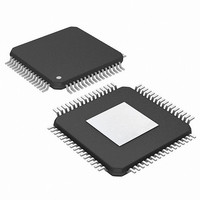
PIC24FJ256DA110-I/PT Microchip Technology, PIC24FJ256DA110-I/PT Datasheet - Page 219

PIC24FJ256DA110-I/PT
Manufacturer Part Number
PIC24FJ256DA110-I/PT
Description
MCU PIC 16BIT FLASH 256K 100TQFP
Manufacturer
Microchip Technology
Series
PIC® 24Fr
Specifications of PIC24FJ256DA110-I/PT
Program Memory Type
FLASH
Program Memory Size
256KB (85.5K x 24)
Package / Case
100-TFQFP
Core Processor
PIC
Core Size
16-Bit
Speed
32MHz
Connectivity
I²C, IrDA, SPI, UART/USART, USB OTG
Peripherals
Brown-out Detect/Reset, GFX, LVD, POR, PWM, WDT
Number Of I /o
84
Ram Size
24K x 8
Voltage - Supply (vcc/vdd)
2.2 V ~ 3.6 V
Data Converters
A/D 24x10b
Oscillator Type
Internal
Operating Temperature
-40°C ~ 85°C
Processor Series
PIC24FJ
Core
PIC
Data Bus Width
16 bit
Data Ram Size
24 KB
Interface Type
UART, SPI, USB, I2C, RS-485, RS-232
Maximum Clock Frequency
32 MHz
Number Of Programmable I/os
23
Number Of Timers
5
Operating Supply Voltage
3.6 V
Maximum Operating Temperature
+ 85 C
Mounting Style
SMD/SMT
3rd Party Development Tools
52713-733, 52714-737, 53276-922, EWDSPIC
Development Tools By Supplier
PG164130, DV164035, DV244005, DV164005, AC164127-4, AC164127-6, AC164139, DM240001, DM240312, DV164039
Minimum Operating Temperature
- 40 C
Controller Family/series
PIC24
No. Of I/o's
84
Ram Memory Size
24KB
Cpu Speed
32MHz
No. Of Timers
5
Embedded Interface Type
I2C, SPI, UART, USB
Rohs Compliant
Yes
Lead Free Status / RoHS Status
Lead free / RoHS Compliant
Eeprom Size
-
Lead Free Status / Rohs Status
Lead free / RoHS Compliant
Available stocks
Company
Part Number
Manufacturer
Quantity
Price
Company:
Part Number:
PIC24FJ256DA110-I/PT
Manufacturer:
Microchip Technology
Quantity:
10 000
- Current page: 219 of 408
- Download datasheet (4Mb)
FIGURE 15-3:
FIGURE 15-4:
2010 Microchip Technology Inc.
Note 1:
Note 1: Using the SSx pin in Slave mode of operation is optional.
Processor 1 (SPI Enhanced Buffer Master)
2:
2: User must write transmit data to read received data from SPIxBUF. The SPIxTXB and SPIxRXB registers are
MSTEN (SPIxCON1<5>) = 1 and
Using the SSx pin in Slave mode of operation is optional.
User must write transmit data to read received data from SPIxBUF. The SPIxTXB and SPIxRXB registers are
memory mapped to SPIxBUF.
SPIBEN (SPIxCON2<0>) = 1
MSTEN (SPIxCON1<5>) = 1)
memory mapped to SPIxBUF.
Processor 1 (SPI Master)
MSb
8-Level FIFO Buffer
MSb
SPI MASTER/SLAVE CONNECTION (STANDARD MODE)
SPI MASTER/SLAVE CONNECTION (ENHANCED BUFFER MODES)
Serial Transmit Buffer
Serial Receive Buffer
Shift Register
(SPIxBUF)
SPIx Buffer
(SPIxSR)
Shift Register
(SPIxBUF)
SPIx Buffer
(SPIxRXB)
(SPIxTXB)
(SPIxSR)
(2)
(2)
LSb
LSb
SDOx
SCKx
SDIx
SDOx
SDIx
SCKx
PIC24FJ256DA210 FAMILY
SSx
Serial Clock
Serial Clock
SSEN (SPIxCON1<7>) = 1 and MSTEN (SPIxCON1<5>) = 0
SDIx
SDOx
SCKx
SSx
SDIx
SDOx
SCKx
SSx
Processor 2 (SPI Enhanced Buffer Slave)
(1)
(1)
MSb
Serial Transmit Buffer
MSTEN (SPIxCON1<5>) = 0 and
Serial Receive Buffer
Processor 2 (SPI Slave)
SPIBEN (SPIxCON2<0>) = 1
SSEN (SPIxCON1<7>) = 1,
Shift Register
(SPIxRXB)
(SPIxBUF)
(SPIxTXB)
(SPIxSR)
SPIx Buffer
MSb
8-Level FIFO Buffer
Shift Register
(SPIxBUF)
SPIx Buffer
(SPIxSR)
(2)
(2)
(2)
(2)
LSb
(2)
LSb
DS39969B-page 219
Related parts for PIC24FJ256DA110-I/PT
Image
Part Number
Description
Manufacturer
Datasheet
Request
R

Part Number:
Description:
Manufacturer:
Microchip Technology Inc.
Datasheet:

Part Number:
Description:
Manufacturer:
Microchip Technology Inc.
Datasheet:

Part Number:
Description:
Manufacturer:
Microchip Technology Inc.
Datasheet:

Part Number:
Description:
Manufacturer:
Microchip Technology Inc.
Datasheet:

Part Number:
Description:
Manufacturer:
Microchip Technology Inc.
Datasheet:

Part Number:
Description:
Manufacturer:
Microchip Technology Inc.
Datasheet:

Part Number:
Description:
Manufacturer:
Microchip Technology Inc.
Datasheet:

Part Number:
Description:
Manufacturer:
Microchip Technology Inc.
Datasheet:


