ATSAM3S2AA-MU Atmel, ATSAM3S2AA-MU Datasheet - Page 25
ATSAM3S2AA-MU
Manufacturer Part Number
ATSAM3S2AA-MU
Description
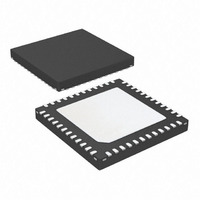
IC MCU 32BIT 128KB FLASH 48QFN
Manufacturer
Atmel
Series
SAM3Sr
Specifications of ATSAM3S2AA-MU
Core Processor
ARM® Cortex-M3™
Core Size
32-Bit
Speed
64MHz
Connectivity
I²C, MMC, SPI, SSC, UART/USART, USB
Peripherals
Brown-out Detect/Reset, DMA, I²S, POR, PWM, WDT
Number Of I /o
34
Program Memory Size
128KB (128K x 8)
Program Memory Type
FLASH
Ram Size
32K x 8
Voltage - Supply (vcc/vdd)
1.62 V ~ 1.95 V
Data Converters
A/D 8x10/12b
Oscillator Type
Internal
Operating Temperature
-40°C ~ 85°C
Package / Case
48-VQFN Exposed Pad, 48-HVQFN, 48-SQFN, 48-DHVQFN
Processor Series
ATSAM3x
Core
ARM Cortex M3
3rd Party Development Tools
JTRACE-CM3, MDK-ARM, RL-ARM, ULINK2
Development Tools By Supplier
ATSAM3S-EK
Lead Free Status / RoHS Status
Lead free / RoHS Compliant
Eeprom Size
-
Lead Free Status / Rohs Status
Details


Table 6-1.
Notes:
6.2.1
6500CS–ATARM–24-Jan-11
SYSTEM_IO
bit number
1. If PB12 is used as PIO input in user applications, a low level must be ensured at startup to prevent Flash erase before the
2. In the product Datasheet Refer to: Slow Clock Generator of the Supply Controller section.
3. In the product Datasheet Refer to: 3 to 20 MHZ Crystal Oscillator information in PMC section.
12
10
11
7
6
5
4
-
-
-
-
Serial Wire JTAG Debug Port (SWJ-DP) Pins
user application sets PB12 into PIO mode,
System I/O Configuration Pin List.
TDO/TRACESWO
Default function
TCK/SWCLK
TMS/SWDIO
The SWJ-DP pins are TCK/SWCLK, TMS/SWDIO, TDO/SWO, TDI and commonly provided on
a standard 20-pin JTAG connector defined by ARM. For more details about voltage reference
and reset state, refer to
At startup, SWJ-DP pins are configured in SWJ-DP mode to allow connection with debugging
probe. Please refer to the Debug and Test Section of the product datasheet.
SWJ-DP pins can be used as standard I/Os to provide users more general input/output pins
when the debug port is not needed in the end application. Mode selection between SWJ-DP
mode (System IO mode) and general IO mode is performed through the AHB Matrix Special
Function Registers (MATRIX_SFR). Configuration of the pad for pull-up, triggers, debouncing
and glitch filters is possible regardless of the mode.
The JTAGSEL pin is used to select the JTAG boundary scan when asserted at a high level. It
integrates a permanent pull-down resistor of about 15 kΩ to GND, so that it can be left uncon-
nected for normal operations.
By default, the JTAG Debug Port is active. If the debugger host wants to switch to the Serial
Wire Debug Port, it must provide a dedicated JTAG sequence on TMS/SWDIO and
TCK/SWCLK which disables the JTAG-DP and enables the SW-DP. When the Serial Wire
Debug Port is active, TDO/TRACESWO can be used for trace.
The asynchronous TRACE output (TRACESWO) is multiplexed with TDO. So the asynchronous
trace can only be used with SW-DP, not JTAG-DP. For more information about SW-DP and
JTAG-DP switching, please refer to the Debug and Test Section.
after reset
ERASE
DDM
DDP
PB9
PB8
PA7
PA8
TDI
Other function
XOUT32
Table 3-1 on page
PB12
PB10
PB11
XIN32
XOUT
PB7
PB6
PB5
PB4
XIN
Low Level at startup
Constraints for
6.
normal start
-
-
-
-
-
-
-
-
-
-
(1)
(Refer to the SystemIO Configuration
Register in the Bus Matrix section of
SAM3S Summary
In Matrix User Interface Registers
the product datasheet.)
See footnote
See footnote
Configuration
(2)
(3)
below
below
25
Related parts for ATSAM3S2AA-MU
Image
Part Number
Description
Manufacturer
Datasheet
Request
R

Part Number:
Description:
KIT EVAL FOR ATSAM3S4C
Manufacturer:
Atmel
Datasheet:
Part Number:
Description:
Development Boards & Kits - ARM EVAL KIT SAM3S8 & SAM3SD8 series
Manufacturer:
Atmel
Datasheet:

Part Number:
Description:
AT91 ARM Cortex M3-based Processor
Manufacturer:
ATMEL [ATMEL Corporation]
Datasheet:

Part Number:
Description:
DEV KIT FOR AVR/AVR32
Manufacturer:
Atmel
Datasheet:

Part Number:
Description:
INTERVAL AND WIPE/WASH WIPER CONTROL IC WITH DELAY
Manufacturer:
ATMEL Corporation
Datasheet:
Part Number:
Description:
Low-Voltage Voice-Switched IC for Hands-Free Operation
Manufacturer:
ATMEL Corporation
Datasheet:
Part Number:
Description:
MONOLITHIC INTEGRATED FEATUREPHONE CIRCUIT
Manufacturer:
ATMEL Corporation
Datasheet:
Part Number:
Description:
AM-FM Receiver IC U4255BM-M
Manufacturer:
ATMEL Corporation
Datasheet:
Part Number:
Description:
Monolithic Integrated Feature Phone Circuit
Manufacturer:
ATMEL Corporation
Datasheet:
Part Number:
Description:
Multistandard Video-IF and Quasi Parallel Sound Processing
Manufacturer:
ATMEL Corporation
Datasheet:
Part Number:
Description:
High-performance EE PLD
Manufacturer:
ATMEL Corporation
Datasheet:
Part Number:
Description:
8-bit Flash Microcontroller
Manufacturer:
ATMEL Corporation
Datasheet: