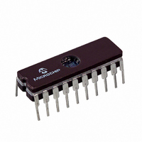
PIC16C432/JW Microchip Technology, PIC16C432/JW Datasheet - Page 25

PIC16C432/JW
Manufacturer Part Number
PIC16C432/JW
Description
IC MCU CMOS 8BIT 20MHZ 2K 20CDIP
Manufacturer
Microchip Technology
Series
PIC® 16Cr
Specifications of PIC16C432/JW
Core Processor
PIC
Core Size
8-Bit
Speed
20MHz
Connectivity
LIN (Local Interconnect Network)
Peripherals
Brown-out Detect/Reset, POR, WDT
Number Of I /o
12
Program Memory Size
3.5KB (2K x 14)
Program Memory Type
EPROM, UV
Ram Size
128 x 8
Voltage - Supply (vcc/vdd)
4.5 V ~ 5.5 V
Oscillator Type
External
Operating Temperature
0°C ~ 70°C
Package / Case
20-CDIP (0.300", 7.62mm) Window
For Use With
AC164029 - MODULE SKT PROMATEII 20DIP/SSOPDVA16XP201 - ADAPTER DEVICE FOR MPLAB-ICE
Lead Free Status / RoHS Status
Contains lead / RoHS non-compliant
Eeprom Size
-
Data Converters
-
5.0
The PIC16C432 has an integrated LIN transceiver
which allows the microcontroller to communicate via
LIN. The LIN protocol is handled by the microcontroller.
The conversion from 5V signal to LIN signals is han-
dled by the transceiver.
5.1
The LIN protocol is not described within this document.
For further information regarding the LIN protocol,
please refer to www.lin-subbus.org.
5.2
The LIN protocol is implemented and programmed by
the user, using the LINTX and LINRX bits, which are
used to interface to the transceiver. The LIN firmware
transmits by toggling the LINTX bit in the LININTF reg-
ister and is read by reading the LINRX bit in the PORTA
register. All aspects of the protocol are handled by soft-
ware (i.e., bit-banged), where the transceiver is used
as the physical interface to the LIN network.
For LIN software implementation, please refer to Micro-
chip’s website (www.microchip.com).
If the LINTX bit is left cleared, no other nodes on the
network will be able to communicate on the LIN for this
is the dominate state for the protocol. The transceiver
can be powered down by clearing the LINVDD bit in the
LININTF register. This can be useful to reduce current
consumption but does not allow the microcontroller to
wake-up on LIN activity because the transceiver will be
disabled. It is recommended that the firmware verify
each bit transmitted, by comparing the LINTX and
LINRX bits, to ensure no bus contention or hardware
failure has occurred. The LINTX bit has no associated
TRIS bit and is always an output. The LINRX bit has an
associated TRIS bit, TLINRX, in the TRISA register.
5.3
Figure 6-1 shows how to implement a hardware LIN
interface in a master configuration and Figure 6-2 in a
slave configuration using the PIC16C432. Figure 6-3
shows how to implement the hardware for a master
configuration using BACT pin to generate a wake-up
interrupt using RB0. The transceiver has an internal
series resistor and diode, as defined in the LIN 1.2
specification, connecting V
Note:
Note:
Note:
2002 Microchip Technology Inc.
LIN TRANSCEIVER
The LIN Protocol
LIN Interfacing
LIN Hardware Interface
The LINTX is bit 2 of the LININTF register.
TLINRX, bit 1 of TRISA register, must be
set to ’1’ at all times.
No resistor is required between V
and 12V supply and for slave configura-
tion, no resistor is required between V
and LIN.
BAT
and LIN.
BAT
BAT
pin
Preliminary
5.4
In thermal shutdown, the LIN output is disabled instan-
taneously. The output transistor is turned off, regard-
less of the input level at pin LINTX bit and only a limited
current can flow into the receiver connected to the LIN
pin.
5.5
The PIC16C432 can wake-up from SLEEP upon bus
activity in two ways:
1.
2.
In case the comparators are used to wake-up the
device upon bus activity, a reference to the LIN signal
has to be supplied. This is usually V
ence can either be an external reference or the internal
voltage reference. Once the device is in SLEEP mode,
the comparator interrupt will wake-up the device. On
RESET, LINRX is configured as an analog comparator
input (Section 8.1 of Data Sheet) which can be used to
generate an interrupt to wake-up the device from
SLEEP on bus activity. The LINRX bit will not receive
data from the bus configured as an analog input, there-
fore, after wake-up from comparator interrupt or
RESET, LINRX must be configured as a digital input to
read the bus.
The BACT output is a CMOS-levels representation of
the LIN pin. This signal can be routed to one of the
PORTB<0,4:7> pins. The RB0/INT external interrupt or
PORTB<4:7> interrupt-on-change wakes up the device
from SLEEP. Any one of the five PORTB pins can be
used for wake-up where PORTB<0> offers multiple
configuration options (Section 10.5.1 of Data Sheet)
and PORTB<4:7> are interrupt-on-change (Section
10.5.3 of Data Sheet).
Note:
Connecting BACT to one of PORTB<0,4:7>
pins.
With the use of the comparators.
Thermal Shutdown
Wake-up From SLEEP Upon Bus
Activity
BACT pin is an output and must be left
open if unused.
PIC16C432
DS41140B-page 23
DD
/2. The refer-


