AT91SAM9263B-CU Atmel, AT91SAM9263B-CU Datasheet
AT91SAM9263B-CU
Specifications of AT91SAM9263B-CU
Available stocks


Related parts for AT91SAM9263B-CU


AT91SAM9263B-CU Summary of contents
Page 1
... Periodic Interval Timer, Watchdog Timer and Double Real-time Timer ® ® Thumb Processor ® ® Technology for Java Acceleration ™ AT91 ARM Thumb Microcontrollers AT91SAM9263 Preliminary Summary NOTE: This is a summary document. The complete document is available on the Atmel website at www.atmel.com. 6249HS–ATARM–27-Jul-09 ...
Page 2
... Three External Clock Inputs, Two Multi-purpose I/O Pins per Channel – Double PWM Generation, Capture/Waveform Mode, Up/Down Capability • One Four-channel 16-bit PWM Controller (PWMC) • One Two-wire Interface (TWI) – Master Mode Support, All Two-wire Atmel AT91SAM9263 Preliminary 2 ™ Compliant ® ...
Page 3
IEEE 1149.1 JTAG Boundary Scan on All Digital Pins • Required Power Supplies – 1.08V to 1.32V for VDDCORE and VDDBU – 3.0V to 3.6V for VDDOSC and VDDPLL – 2.7V to 3.6V for VDDIOP0 (Peripheral I/Os) – ...
Page 4
AT91SAM9263 Block Diagram Figure 2-1. AT91SAM9263 Block Diagram AT91SAM9263 Preliminary 4 6249HS–ATARM–27-Jul-09 ...
Page 5
Signal Description Table 3-1 Table 3-1. Signal Description List Signal Name Function VDDIOM0 EBI0 I/O Lines Power Supply VDDIOM1 EBI1 I/O Lines Power Supply VDDIOP0 Peripherals I/O Lines Power Supply VDDIOP1 Peripherals I/O Lines Power Supply VDDBU Backup I/O ...
Page 6
Table 3-1. Signal Description List (Continued) Signal Name Function TSYNC Trace Synchronization Signal TCLK Trace Clock TPS0 - TPS2 Trace ARM Pipeline Status TPK0 - TPK15 Trace Packet Port NRST Microcontroller Reset TST Test Mode Select BMS Boot Mode Select ...
Page 7
Table 3-1. Signal Description List (Continued) Signal Name Function EBI0_CFCE1 - EBI0_CFCE2 CompactFlash Chip Enable EBI0_CFOE CompactFlash Output Enable EBI0_CFWE CompactFlash Write Enable EBI0_CFIOR CompactFlash IO Read EBI0_CFIOW CompactFlash IO Write EBI0_CFRNW CompactFlash Read Not Write EBI0_CFCS0 - EBI0_CFCS1 CompactFlash ...
Page 8
Table 3-1. Signal Description List (Continued) Signal Name Function TKx SSCx Transmit Clock RKx SSCx Receive Clock TFx SSCx Transmit Frame Sync RFx SSCx Receive Frame Sync AC97RX AC97 Receive Signal AC97TX AC97 Transmit Signal AC97FS AC97 Frame Synchronization Signal ...
Page 9
Table 3-1. Signal Description List (Continued) Signal Name Function ETXCK Transmit Clock or Reference Clock ERXCK Receive Clock ETXEN Transmit Enable ETX0-ETX3 Transmit Data ETXER Transmit Coding Error ERXDV Receive Data Valid ERX0-ERX3 Receive Data ERXER Receive Error ECRS Carrier ...
Page 10
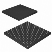
Package and Pinout The AT91SAM9263 is available in a 324-ball TFBGA Green package mm, 0.8mm ball pitch. 4.1 324-ball TFBGA Package Outline Figure 4-1 A detailed mechanical description is given in the section “AT91SAM9263 Mechanical Character- ...
Page 11
TFBGA Package Pinout Table 4-1. AT91SAM9263 Pinout for 324-ball TFBGA Package Pin Signal Name Pin A1 EBI0_D2 E10 A2 EBI0_SDCKE E11 A3 EBI0_NWE_NWR0 E12 A4 EBI0_NCS1_SDCS E13 A5 EBI0_A19 E14 A6 EBI0_A11 E15 A7 EBI0_A10 E16 A8 EBI0_A5 ...
Page 12
Table 4-1. AT91SAM9263 Pinout for 324-ball TFBGA Package (Continued) Pin Signal Name Pin C15 PC3 H6 C16 GND H7 C17 VDDIOP0 H8 C18 HDPB H9 D1 EBI0_D10 H10 D2 EBI0_D3 H11 ( H12 D4 EBI0_D1 H13 D5 EBI0_A20 ...
Page 13
Power Considerations 5.1 Power Supplies AT91SAM9263 has several types of power supply pins: • VDDCORE pins: Power the core, including the processor, the embedded memories and the peripherals; voltage ranges from 1.08V to 1.32V, 1.2V nominal. • VDDIOM0 and ...
Page 14
EBI0 voltage range. The user must be sure to program the EBI0 voltage range before getting the device out of its Slow Clock Mode. 6. I/O Line Considerations 6.1 JTAG Port Pins ...
Page 15
MΩ. The resistor value is calculated according to the regulator enable implementation and the SHDN level. The pin WKUP is an input-only. It can accept voltages only between 0V and VDDBU. 7. Processor and Architecture 7.1 ARM926EJ-S Processor • RISC ...
Page 16
Bus Matrix • 9-layer Matrix, handling requests from 9 masters • Programmable Arbitration strategy – Fixed-priority Arbitration – Round-Robin Arbitration, either with no default master, last accessed default master • Burst Management – Breaking with Slot Cycle Limit Support ...
Page 17
The LCD Controller, the DMA Controller, the USB OTG and the USB Host have a user interface mapped as a slave on the Matrix. They share the same layer, as programming them does not require a high bandwidth. Table 7-2. ...
Page 18
Master to Slave Access In most cases, all the masters can access all the slaves. However, some paths do not make sense, for example, allowing access from the Ethernet MAC to the Internal Peripherals. Thus, these paths are forbidden ...
Page 19
USART1 Transmit Channel – USART0 Transmit Channel – AC97 Transmit Channel – SPI1 Transmit Channel – SPI0 Transmit Channel – SSC1 Transmit Channel – SSC0 Transmit Channel – DBGU Receive Channel – USART2 Receive Channel – USART1 Receive Channel ...
Page 20
Suspend DMA operation – Programmable DMA lock transfer support. • Transfer Initiation – Supports four external DMA Requests – Support for software handshaking interface. Memory mapped registers can be used • Interrupt – Programmable interrupt generation on DMA transfer ...
Page 21
Memories Figure 8-1. AT91SAM9263 Memory Mapping Address Memory Space 0x0000 0000 Internal Memories 0x0FFF FFFF 0x1000 0000 EBI0 Chip Select 0 0x1FFF FFFF 0x2000 0000 EBI0 Chip Select 1/ EBI0 SDRAMC 0x2FFF FFFF 0x3000 0000 EBI0 Chip Select 2 ...
Page 22
A first level of address decoding is performed by the Bus Matrix, i.e., the implementation of the Advanced High Performance Bus (AHB) for its master and slave interfaces with additional features. Decoding breaks up the 4G bytes of address space ...
Page 23
Chip Configuration User Interface. This SRAM block is also accessible by the ARM926 Data Master and by the AHB Masters through the AHB bus at address 0x0010 0000. • Internal SRAM B is the ARM926EJ-S ...
Page 24
Table 8-3. 16 Kbyte Block Allocation (Continued) Configuration examples and related 16 Kbyte block assignments ITCM = 0 Kbyte Decoded DTCM = 0 Kbyte Area Address AHB = 80 Kbytes 0x0030 0000 0x0030 4000 Internal SRAM C 0x0030 8000 (AHB) ...
Page 25
SD Card – NAND Flash – SPI DataFlash • Interface with SAM-BA – Serial communication on a DBGU – USB Bulk Device Port 8.1.2.2 BMS = 0, Boot on External Memory • Boot at slow clock • Boot with ...
Page 26
External Bus Interface 1 • Integrates three External Memory Controllers: – Static Memory Controller – SDRAM Controller – ECC Controller • Additional logic for NAND Flash • Optional Full 32-bit External Data Bus • 23-bit Address Bus ...
Page 27
Energy-saving capabilities – Self-refresh, power down and deep power down modes supported • Error detection – Refresh Error Interrupt • SDRAM Power-up Initialization by software • CAS Latency and 3 supported • Auto Precharge Command not ...
Page 28
System Controller Block Diagram Figure 9-1. AT91SAM9263 System Controller Block Diagram irq0-irq1 periph_irq[2..29] pit_irq rtt0_irq rtt1_irq wdt_irq dbgu_irq pmc_irq rstc_irq periph_nreset dbgu_rxd debug periph_nreset SLCK debug proc_nreset NRST VDDCORE POR VDDCORE VDDBU VDDBU POR SLCK SLCK backup_nreset SLCK backup_nreset ...
Page 29
Reset Controller • Based on two Power-on-Reset cells – One on VDDBU and one on VDDCORE • Status of the last reset – Either general reset (VDDBU rising), wake-up reset (VDDCORE rising), software • Controls the internal resets and ...
Page 30
Power Management Controller • Provides: – the Processor Clock PCK – the Master Clock MCK, in particular to the Matrix and the memory interfaces – the USB Device Clock UDPCK – the USB Host Clock UHPCK – independent peripheral ...
Page 31
Windowed, prevents the processor deadlocking on the watchdog access 9.8 Real-time Timer • Two Real-time Timers, allowing backup of time with different accuracies – 32-bit Free-running back-up counter – Integrates a 16-bit programmable prescaler running on the embedded 32.768Hz ...
Page 32
... Implemented features are 100% compatible with the standard Atmel USART – Independent receiver and transmitter with a common programmable Baud Rate – Even, Odd, Mark or Space Parity Generation – Parity, Framing and Overrun Error Detection – Automatic Echo, Local Loopback and Remote Loopback Channel Modes – ...
Page 33
Peripherals 10.1 User Interface The Peripherals are mapped in the upper 256 Mbytes of the address space between the addresses 0xFFFA 0000 and 0xFFFC FFFF. Each User Peripheral is allocated 16 Kbytes of address space. A complete memory map ...
Page 34
Table 10-1. AT91SAM9263 Peripheral Identifiers (Continued) Peripheral ID Peripheral Mnemonic 29 UHP 30 AIC 31 AIC Note: Setting AIC, SYSC, UHP and IRQ0 - 1 bits in the clock set/clear registers of the PMC has no effect. 10.2.1 Peripheral Interrupts ...
Page 35
As a result, the bit corresponding to the PIO Line in the register PIO_PSR (Peripheral Status Register) resets low signal name is specified in the ...
Page 36
PIO Controller A Multiplexing Table 10-2. Multiplexing on PIO Controller A PIO Controller A I/O Line Peripheral A PA0 MCI0_DA0 PA1 MCI0_CDA PA2 PA3 MCI0_DA1 PA4 MCI0_DA2 PA5 MCI0_DA3 PA6 MCI1_CK PA7 MCI1_CDA PA8 MCI1_DA0 PA9 MCI1_DA1 PA10 MCI1_DA2 ...
Page 37
PIO Controller B Multiplexing Table 10-3. Multiplexing on PIO Controller B PIO Controller B I/O Line Peripheral A PB0 AC97FS PB1 AC97CK PB2 AC97TX PB3 AC97RX PB4 TWD PB5 TWCK PB6 TF1 PB7 TK1 PB8 TD1 PB9 RD1 PB10 ...
Page 38
PIO Controller C Multiplexing Table 10-4. Multiplexing on PIO Controller C PIO Controller C I/O Line Peripheral A PC0 LCDVSYNC PC1 LCDHSYNC PC2 LCDDOTCK PC3 LCDDEN PC4 LCDD0 PC5 LCDD1 PC6 LCDD2 PC7 LCDD3 PC8 LCDD4 PC9 LCDD5 PC10 ...
Page 39
PIO Controller D Multiplexing Table 10-5. Multiplexing on PIO Controller D PIO Controller D I/O Line Peripheral A PD0 TXD1 PD1 RXD1 PD2 TXD2 PD3 RXD2 PD4 FIQ PD5 EBI0_NWAIT PD6 EBI0_NCS4/CFCS0 PD7 EBI0_NCS5/CFCS1 PD8 EBI0_CFCE1 PD9 EBI0_CFCE2 PD10 ...
Page 40
PIO Controller E Multiplexing Table 10-6. Multiplexing on PIO Controller E PIO Controller E I/O Line Peripheral A PE0 ISI_D0 PE1 ISI_D1 PE2 ISI_D2 PE3 ISI_D3 PE4 ISI_D4 PE5 ISI_D5 PE6 ISI_D6 PE7 ISI_D7 PE8 ISI_PCK PE9 ISI_HSYNC PE10 ...
Page 41
System Resource Multiplexing 10.4.1 LCD Controller The LCD Controller can interface with several LCD panels. It supports 4 bits per pixel (bpp), 8 bpp or 16 bpp without limitation. Interfacing 24 bpp TFT panels prevents using the Ethernet MAC. ...
Page 42
CompactFlash Using the CompactFlash interface prevents using NCS4 and/or NCS5 to access other parallel devices. 10.4.9 SPI0 and MCI Interface SPI0 signals and MCI0 signals are multiplexed, as the DataFlash Card is hardware-compatible with the SDCard. Only one can ...
Page 43
USART • Programmable Baud Rate Generator • 9-bit full-duplex synchronous or asynchronous serial communications – stop bits in Asynchronous Mode stop bits in Synchronous Mode – Parity generation and ...
Page 44
Timer Counter • Three 16-bit Timer Counter Channels • Wide range of functions including: – Frequency Measurement – Event Counting – Interval Measurement – Pulse Generation – Delay Timing – Pulse Width Modulation – Up/down Capabilities • Each channel ...
Page 45
Bit rates up to 1Mbit/s. • Object-oriented mailboxes, each with the following properties: – CAN Specification 2.0 Part A or 2.0 Part B programmable for each message – Object Configurable as receive (with overwrite or not) or transmit – ...
Page 46
STN • bits per pixel (palletized), 16, 24 bits per pixel (non-palletized) for TFT • Single clock domain architecture • ...
Page 47
Package Drawing Figure 11-1. 324-ball TFBGA Package Drawing Table 11-1. Soldering Information Ball Land Soldering Mask Opening Table 11-2. Device and 324-ball TFBGA Package Maximum Weight 572 Table 11-3. 324-ball TFBGA Package Characteristics Moisture Sensitivity Level Table 11-4. Package ...
Page 48
... AT91SAM9263 Ordering Information Table 12-1. AT91SAM9263 Ordering Information MLR A Ordering Code MLR B Ordering Code AT91SAM9263-CU AT91SAM9263B-CU AT91SAM9263 Preliminary 48 Package Package Type TFBGA 324 Green Temperature Operating Range Industrial -40°C to 85°C 6249HS–ATARM–27-Jul-09 ...
Page 49
... Section 5.1 ”Power Supplies”, VDDCORE and VDDBU updated. Section 5.2, “Power Sequence Requirements removed from datasheet. 6249ES New Ordering Code: AT91SAM9263B-CU added to Section 8.1.2.1 ”BMS = 1, Boot on Embedded memory” Section 5.2 ”Power Sequence Section 10.4.3 ”EBI1”, System Resource Multiplexing, Ethernet 10/100 MAC limitation on EBI1 updated. ...
Page 50
Table 13-1. Revision History Document Ref. Comments 6249CS In Section 4.1 “324-ball TFBGA Package Outline” on page 10 All new information for Slaves,” on page 17 and In Section 9.3 “Shutdown Controller” on page In Section 5.2 “Power Consumption” on ...
Page 51
... Disclaimer: The information in this document is provided in connection with Atmel products. No license, express or implied, by estoppel or otherwise, to any intellectual property right is granted by this document or in connection with the sale of Atmel products. EXCEPT AS SET FORTH IN ATMEL’S TERMS AND CONDI- TIONS OF SALE LOCATED ON ATMEL’S WEB SITE, ATMEL ASSUMES NO LIABILITY WHATSOEVER AND DISCLAIMS ANY EXPRESS, IMPLIED OR STATUTORY WARRANTY RELATING TO ITS PRODUCTS INCLUDING, BUT NOT LIMITED TO, THE IMPLIED WARRANTY OF MERCHANTABILITY, FITNESS FOR A PARTICULAR PURPOSE, OR NON-INFRINGEMENT ...