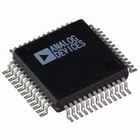
ADUC812BSZ Analog Devices Inc, ADUC812BSZ Datasheet - Page 8

ADUC812BSZ
Manufacturer Part Number
ADUC812BSZ
Description
IC ADC 12BIT MULTICH MCU 52-MQFP
Manufacturer
Analog Devices Inc
Series
MicroConverter® ADuC8xxr
Datasheet
1.EVAL-ADUC812QS.pdf
(60 pages)
Specifications of ADUC812BSZ
Core Size
8-Bit
Program Memory Size
8KB (8K x 8)
Core Processor
8052
Speed
16MHz
Connectivity
I²C, SPI, UART/USART
Peripherals
PSM, Temp Sensor, WDT
Number Of I /o
34
Program Memory Type
FLASH
Eeprom Size
640 x 8
Ram Size
256 x 8
Voltage - Supply (vcc/vdd)
2.7 V ~ 5.5 V
Data Converters
A/D 8x12b, D/A 2x12b
Oscillator Type
Internal
Operating Temperature
-40°C ~ 85°C
Package / Case
52-MQFP, 52-PQFP
Controller Family/series
(8051) 8052
No. Of I/o's
32
Eeprom Memory Size
8KB
Ram Memory Size
256Byte
Cpu Speed
1.3MIPS
No. Of Timers
3
Package
52MQFP
Device Core
8052
Family Name
ADuC8xx
Maximum Speed
16 MHz
Operating Supply Voltage
3.3|5 V
Data Bus Width
8 Bit
Number Of Programmable I/os
32
Interface Type
I2C/SPI/TWI/UART
On-chip Adc
8-chx12-bit
On-chip Dac
2-chx12-bit
Number Of Timers
3
Lead Free Status / RoHS Status
Lead free / RoHS Compliant
Available stocks
Company
Part Number
Manufacturer
Quantity
Price
Company:
Part Number:
ADUC812BSZ
Manufacturer:
ADI
Quantity:
2 400
Company:
Part Number:
ADUC812BSZ
Manufacturer:
Analog Devices Inc
Quantity:
10 000
Part Number:
ADUC812BSZ
Manufacturer:
ADI/亚德诺
Quantity:
20 000
Company:
Part Number:
ADUC812BSZ-REEL
Manufacturer:
Analog Devices Inc
Quantity:
10 000
ADuC812
Mnemonic
PSEN
ALE
EA
P0.7–P0.0
(A0–A7)
TERMINOLOGY
ADC SPECIFICATIONS
Integral Nonlinearity
This is the maximum deviation of any code from a straight line
passing through the endpoints of the ADC transfer function.
The endpoints of the transfer function are zero scale, a point
1/2 LSB below the first code transition, and full scale, a point
1/2 LSB above the last code transition.
Differential Nonlinearity
This is the difference between the measured and the ideal 1 LSB
change between any two adjacent codes in the ADC.
Offset Error
This is the deviation of the first code transition (0000 . . . 000)
to (0000 . . . 001) from the ideal, i.e., +1/2 LSB.
Full-Scale Error
This is the deviation of the last code transition from the ideal
AIN voltage (Full Scale – 1.5 LSB) after the offset error has
been adjusted out.
Signal-to-(Noise + Distortion) Ratio
This is the measured ratio of signal-to-(noise + distortion) at the
output of the ADC. The signal is the rms amplitude of the fun-
damental. Noise is the rms sum of all nonfundamental signals up
to half the sampling frequency (f
Type Function
O
O
I
I/O
Port 0 is an 8-bit open-drain bidirectional I/O port. Port 0 pins that have 1s written to them float and in
that state can be used as high impedance inputs. Port 0 is also the multiplexed low order address and data
Program Store Enable, Logic Output. This output is a control signal that enables the external program
memory to the bus during external fetch operations. It is active every six oscillator periods except during
external data memory accesses. This pin remains high during internal program execution. PSEN can also be
used to enable serial download mode when pulled low through a resistor on power-up or RESET.
Address Latch Enable, Logic Output. This output is used to latch the low byte (and page byte for 24-bit
address space accesses) of the address into external memory during normal operation. It is activated every
six oscillator periods except during an external data memory access.
External Access Enable, Logic Input. When held high, this input enables the device to fetch code from
internal program memory locations 0000H to 1FFFH. When held low, this input enables the device to fetch
all instructions from external program memory.
bus during accesses to external program or data memory. In this application, it uses strong internal pull-ups
when emitting 1s.
S
/2), excluding dc. The ratio is
PIN FUNCTION DESCRIPTIONS (continued)
–8–
dependent upon the number of quantization levels in the digiti-
zation process; the more levels, the smaller the quantization
noise. The theoretical signal-to-(noise + distortion) ratio for an
ideal N-bit converter with a sine wave input is given by:
Thus for a 12-bit converter, this is 74 dB.
Total Harmonic Distortion
Total Harmonic Distortion is the ratio of the rms sum of the
harmonics to the fundamental.
DAC SPECIFICATIONS
Relative Accuracy
Relative accuracy or endpoint linearity is a measure of the
maximum deviation from a straight line passing through the
endpoints of the DAC transfer function. It is measured after
adjusting for zero-scale error and full-scale error.
Voltage Output Settling Time
This is the amount of time it takes for the output to settle to a
specified level for a full-scale input change.
Digital-to-Analog Glitch Impulse
This is the amount of charge injected into the analog output
when the inputs change state. It is specified as the area of the
glitch in nV sec.
Signal-to-(Noise + Distortion) = (6.02N + 1.76) dB
REV. E


