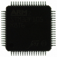
STM32F105R8T6 STMicroelectronics, STM32F105R8T6 Datasheet - Page 34

STM32F105R8T6
Manufacturer Part Number
STM32F105R8T6
Description
MCU ARM 64KB FLASH MEM 64-LQFP
Manufacturer
STMicroelectronics
Series
STM32r
Specifications of STM32F105R8T6
Core Processor
ARM® Cortex-M3™
Core Size
32-Bit
Speed
72MHz
Connectivity
CAN, Ethernet, I²C, IrDA, LIN, SPI, UART/USART, USB OTG
Peripherals
DMA, POR, PWM, Voltage Detect, WDT
Number Of I /o
51
Program Memory Size
64KB (64K x 8)
Program Memory Type
FLASH
Ram Size
20K x 8
Voltage - Supply (vcc/vdd)
2 V ~ 3.6 V
Data Converters
A/D 16x12b; D/A 2x12b
Oscillator Type
Internal
Operating Temperature
-40°C ~ 85°C
Package / Case
64-LQFP
Processor Series
STM32F105x
Core
ARM Cortex M3
Data Bus Width
32 bit
Data Ram Size
20 KB
Interface Type
CAN, I2C, SPI, USART
Maximum Clock Frequency
72 MHz
Number Of Programmable I/os
51
Number Of Timers
10
Operating Supply Voltage
2 V to 3.6 V
Maximum Operating Temperature
+ 85 C
Mounting Style
SMD/SMT
3rd Party Development Tools
EWARM, EWARM-BL, MDK-ARM, RL-ARM, ULINK2
Minimum Operating Temperature
- 40 C
On-chip Adc
12 bit x 2, 16 Channel
On-chip Dac
12 bit x 2, 2 Channel
Cpu Family
STM32
Device Core
ARM Cortex-M3
Device Core Size
32b
Frequency (max)
72MHz
Total Internal Ram Size
20KB
# I/os (max)
51
Number Of Timers - General Purpose
7
Operating Supply Voltage (typ)
2.5/3.3V
Operating Supply Voltage (max)
3.6V
Operating Supply Voltage (min)
2V
Instruction Set Architecture
RISC
Operating Temp Range
-40C to 85C
Operating Temperature Classification
Industrial
Mounting
Surface Mount
Pin Count
64
Package Type
LQFP
For Use With
497-10591 - DAUGHTER BOARD FOR STM32497-9040 - DEV KIT FOR STM32497-9041 - DEV KIT FOR STM32497-9042 - DEV KIT FOR STM32497-9043 - DEV KIT FOR STM32497-8924 - EVAL BOARD FOR STM32F107VCT497-8853 - BOARD DEMO STM32 UNIV USB-UUSCI
Lead Free Status / RoHS Status
Lead free / RoHS Compliant
Eeprom Size
-
Lead Free Status / Rohs Status
Lead free / RoHS Compliant
Other names
497-8922
Available stocks
Company
Part Number
Manufacturer
Quantity
Price
Company:
Part Number:
STM32F105R8T6
Manufacturer:
AIMTEC
Quantity:
3 000
Company:
Part Number:
STM32F105R8T6
Manufacturer:
STMicroelectronics
Quantity:
10 000
Part Number:
STM32F105R8T6
Manufacturer:
ST
Quantity:
20 000
Electrical characteristics
5.2
34/101
Absolute maximum ratings
Stresses above the absolute maximum ratings listed in
Table 7: Current
damage to the device. These are stress ratings only and functional operation of the device
at these conditions is not implied. Exposure to maximum rating conditions for extended
periods may affect device reliability.
Table 6.
1. All main power (V
2. I
Table 7.
1. All main power (V
2. I
3. Negative injection disturbs the analog performance of the device. See note in
4. When several inputs are submitted to a current injection, the maximum I
|V
V
I
V
INJ(PIN)
I
supply, in the permitted range.
maximum is respected. If V
externally to the I
induced by V
supply, in the permitted range.
cannot be respected, the injection current must be limited externally to the I
injection is induced by V
characteristics.
positive and negative injected currents (instantaneous values). These results are based on
characterization with I
Symbol
SSX
INJ(PIN)
INJ(PIN)
|V
ESD(HBM)
DD
Symbol
INJ(PIN)
V
I
I
–V
VDD
DDx
VSS
I
IN
V
IO
SS
must never be exceeded (see
(2)(3)
must never be exceeded. This is implicitly insured if V
|
SS
(2)
|
Voltage characteristics
Current characteristics
IN
External main supply voltage (including V
and V
Input voltage on five volt tolerant pin
Input voltage on any other pin
Variations between different V
Variations between all the different ground pins
Electrostatic discharge voltage (human body
model)
< V
characteristics, and
Total current into V
Total current out of V
Output current sunk by any I/O and control pin
Output current source by any I/Os and control pin
Injected current on NRST pin
Injected current on HSE OSC_IN and LSE OSC_IN pins
Injected current on any other pin
Total injected current (sum of all I/O and control pins)
INJ(PIN)
DD
DD
SS
, V
, V
DD
.
DDA
DDA
INJ(PIN)
)
IN
value. A positive injection is induced by V
(1)
> V
) and ground (V
) and ground (V
IN
maximum cannot be respected, the injection current must be limited
DD
maximum current injection on four I/O port pins of the device.
while a negative injection is induced by V
Doc ID 15274 Rev 5
Ratings
DD
Table 7: Current
SS
/V
Table 8: Thermal characteristics
SS
SS
DDA
ground lines (sink)
, V
, V
Ratings
SSA
SSA
(2)
power lines (source)
DD
) pins must always be connected to the external power
) pins must always be connected to the external power
power pins
(4)
(2)
characteristics). This is implicitly insured if V
DDA
IN
maximum is respected. If V
(1)
Table 6: Voltage
IN
> V
see
Absolute maximum ratings
(electrical sensitivity)
(1)
STM32F105xx, STM32F107xx
IN
V
V
INJ(PIN)
max while a negative injection is
SS
SS
IN
Section 5.3.11:
–0.3
INJ(PIN)
Min
(4)
< V
0.3
0.3
Section 5.3.16: 12-bit ADC
is the absolute sum of the
SS
may cause permanent
.
value. A positive
characteristics,
V
Max.
25
± 25
150
150
± 5
± 5
± 5
DD
25
Max
+5.5
IN
4.0
50
50
+0.3
maximum
IN
Unit
mA
Unit
mV
V


