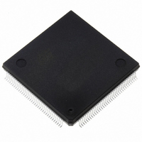
ST10F269Z2Q6 STMicroelectronics, ST10F269Z2Q6 Datasheet - Page 28

ST10F269Z2Q6
Manufacturer Part Number
ST10F269Z2Q6
Description
MCU 16BIT 256K FLASH 144PQFP
Manufacturer
STMicroelectronics
Series
ST10r
Specifications of ST10F269Z2Q6
Core Processor
ST10
Core Size
16-Bit
Speed
40MHz
Connectivity
CAN, EBI/EMI, SSC, UART/USART
Peripherals
POR, PWM, WDT
Number Of I /o
111
Program Memory Size
256KB (256K x 8)
Program Memory Type
FLASH
Ram Size
12K x 8
Voltage - Supply (vcc/vdd)
4.5 V ~ 5.5 V
Data Converters
A/D 16x10b
Oscillator Type
Internal
Operating Temperature
-40°C ~ 85°C
Package / Case
144-QFP
Controller Family/series
ST10
No. Of I/o's
111
Ram Memory Size
12KB
Cpu Speed
40MHz
No. Of Timers
5
Embedded Interface Type
CAN, SSC, USART
Rohs Compliant
Yes
Processor Series
ST10F26x
Core
ST10
Data Bus Width
16 bit
Data Ram Size
12 KB
Interface Type
CAN, SSC, USART
Maximum Clock Frequency
40 MHz
Number Of Programmable I/os
111
Number Of Timers
2 x 16 bit
Operating Supply Voltage
0.3 V to 4 V
Maximum Operating Temperature
+ 85 C
Mounting Style
SMD/SMT
Minimum Operating Temperature
- 40 C
On-chip Adc
16 bit x 10 bit
Lead Free Status / RoHS Status
Lead free / RoHS Compliant
Eeprom Size
-
Lead Free Status / Rohs Status
Details
Other names
497-4833
Available stocks
Company
Part Number
Manufacturer
Quantity
Price
Company:
Part Number:
ST10F269Z2Q6
Manufacturer:
ST
Quantity:
201
Company:
Part Number:
ST10F269Z2Q6
Manufacturer:
ST
Quantity:
745
Company:
Part Number:
ST10F269Z2Q6
Manufacturer:
STMicroelectronics
Quantity:
10 000
Part Number:
ST10F269Z2Q6
Manufacturer:
ST
Quantity:
20 000
5 - INTERNAL FLASH MEMORY
5.5.3 - Programming Examples
Most of the microcontroller programs are written in the C language where the data page pointers are
automatically set by the compiler. But because the C compiler may use the not allowed direct addressing
mode for Flash write addresses, it is necessary to program the organizational Flash accesses (command
sequences) with assembler in-line routines which use indirect addressing.
Example 1 Performing the command Read/Reset
We assume that in the initialization phase the lowest 32K Bytes of Flash memory (sector 0) have been
mapped to segment 1.
According to the usual way of ST10 data addressing with data page pointers, address bit A15 and A14 of
a 16-bit command write address select the data page pointer (DPP) which contains the upper 10-bit for
building the 24-bit physical data address. Address bit A13...A0 represent the address offset. As the bit
A14...A17 are "don’t care" when written a Flash command in the Command Interface (CI), we can choose
the most convenient DPPx register for address handling.
The following examples are making usage of DPP0. We just have to make sure, that DPP0 points to
active Flash memory space.
To be independent of mapping of sector 0 we choose for all DPPs which are used for Flash address
handling, to point to segment 2.
For this reason we load DPP0 with value 08h (00 0000 l000b).
MOV
MOV
SCXT
MOV
MOV
MOV
MOV
MOV
MOV
POP
In the example above the 16-bit registers R5 and R6 are used as auxiliary registers for indirect
addressing.
Example 2 Performing a Program Word command
We assume that in the initialization phase the lowest 32K Bytes of Flash memory (sector 0) have been
mapped to segment 1.The data to be written is loaded in register R13, the address to be programmed is
loaded in register R11/R12 (segment number in R11, segment offset in R12).
MOV
MOV
SXCT
MOV
MOV
MOV
MOV
MOV
MOV
POP
28/184
R5, #01554h
R6, #02AA8h
DPPO, #08h
R7, #0A8h
[R5], R7
R7, #054h
[R6], R7
R7, #0F0h
[R5], R7
DPP0
R5, #01554h
R6, #02AA8h
DPPO, #08h
R7, #0A8h
[R5], R7
R7, #054h
[R6], R7
R7, #0A0h
[R5], R7
DPP0
;load auxilary register R5 with command address
;(used in command cycle 1)
;load auxilary register R6 with command address
;(used in command cycle 2)
;push data page pointer 0 and load it to point to
;segment 2
;load register R7 with 1st CI enable command
;command cycle 1
;load register R7 with 2cd CI enable command
;command cycle 2
;load register R7 with Read/Reset command
;command cycle 3. Address is don’t care
;restore DPP0 value
;load auxilary register R5 with command address
;(used in command cycle 1)
;load auxilary register R6 with command address
;(used in command cycle 2)
;push data page pointer 0 and load it to point to
;segment 2
;load register R7 with 1st CI enable command
;command cycle 1
;load register R7 with 2cd CI enable command
;command cycle 2
;load register R7 with Program Word command
;command cycle 3
;restore DPP0: following addressing to the Flash
;will use EXTended instructions
;R11 contains the segment to be programmed
ST10F269


