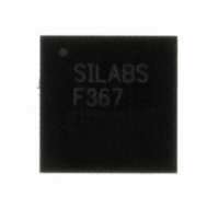
C8051F367-GM Silicon Laboratories Inc, C8051F367-GM Datasheet - Page 28

C8051F367-GM
Manufacturer Part Number
C8051F367-GM
Description
IC 8051 MCU 32K FLASH 28-QFN
Manufacturer
Silicon Laboratories Inc
Series
C8051F36xr
Specifications of C8051F367-GM
Program Memory Type
FLASH
Program Memory Size
32KB (32K x 8)
Package / Case
28-QFN
Core Processor
8051
Core Size
8-Bit
Speed
50MHz
Connectivity
SMBus (2-Wire/I²C), SPI, UART/USART
Peripherals
POR, PWM, Temp Sensor, WDT
Number Of I /o
25
Ram Size
1K x 8
Voltage - Supply (vcc/vdd)
2.7 V ~ 3.6 V
Data Converters
A/D 17x10b; D/A 1x10b
Oscillator Type
Internal
Operating Temperature
-40°C ~ 85°C
Processor Series
C8051F3x
Core
8051
Data Bus Width
8 bit
Data Ram Size
1 KB
Interface Type
I2C/SMBus/SPI/UART
Maximum Clock Frequency
50 MHz
Number Of Programmable I/os
25
Number Of Timers
4
Maximum Operating Temperature
+ 85 C
Mounting Style
SMD/SMT
3rd Party Development Tools
KSK-SL-TOOLSTICK, PK51, CA51, A51, ULINK2
Development Tools By Supplier
C8051F360DK
Minimum Operating Temperature
- 40 C
On-chip Adc
21-ch x 10-bit
On-chip Dac
1-ch x 10-bit
Package
28QFN EP
Device Core
8051
Family Name
C8051F36x
Maximum Speed
50 MHz
Operating Supply Voltage
3 V
Lead Free Status / RoHS Status
Lead free / RoHS Compliant
For Use With
770-1006 - ISP 4PORT FOR SILABS C8051F MCU336-1410 - KIT DEV FOR C8051F360 FAMILY
Eeprom Size
-
Lead Free Status / Rohs Status
Lead free / RoHS Compliant
Other names
336-1649
Available stocks
Company
Part Number
Manufacturer
Quantity
Price
Company:
Part Number:
C8051F367-GM
Manufacturer:
Silicon Labs
Quantity:
135
- Current page: 28 of 288
- Download datasheet (3Mb)
C8051F360/1/2/3/4/5/6/7/8/9
cated by a status bit and an interrupt (if enabled). The resulting 10-bit data word is latched into the ADC
data SFRs upon completion of a conversion.
Window compare registers for the ADC data can be configured to interrupt the controller when ADC data is
either within or outside of a specified range. The ADC can monitor a key voltage continuously in back-
ground mode, but not interrupt the controller unless the converted data is within/outside the specified
range.
1.8.
C8051F36x devices include two on-chip voltage comparators that are enabled/disabled and configured via
user software. Port I/O pins may be configured as comparator inputs via a selection mux. Two comparator
outputs may be routed to a Port pin if desired: a latched output and/or an unlatched (asynchronous) output.
Comparator response time is programmable, allowing the user to select between high-speed and low-
power modes. Positive and negative hysteresis are also configurable.
Comparator interrupts may be generated on rising, falling, or both edges. When in IDLE mode, these inter-
rupts may be used as a “wake-up” source. Comparator0 may also be configured as a reset source.
Figure 1.12 shows the Comparator0 block diagram, and Figure 1.13 shows the Comparator1 block dia-
gram.
Note: The first Port I/O pins shown in Figure 1.12 and Figure 1.13 are for the 48-pin (C8051F360/3)
devices. The second set of Port I/O pins are for the 32-pin and 28-pin (C8051F361/2/4/5/6/7/8/9) devices.
Please refer to the CPTnMX registers (SFR Definition 8.2 and SFR Definition 8.5) for more information.
28
P3.1-3.4 available on
P3.1-3.4 available on
P1.0-1.3 available on
C8051F361/2/6/7/8/9
P1.0-1.3 available on
C8051F361/2/6/7/8/9
C8051F360/1/6/8
C8051F360/1/6/8
Comparators
Sensor
Temp
VREF
GND
VDD
P1.0
P1.7
P2.0
P2.7
P3.0
P3.4
P1.0
P1.7
P2.0
P2.7
P3.0
P3.4
Figure 1.11. 10-Bit ADC Block Diagram
23-to-1
23-to-1
AMUX
AMUX
AMX0P
AMX0N
Rev. 1.0
(+)
(-)
ADC0CF
ADC
10-Bit
VDD
SAR
ADC0GTH ADC0GTL
ADC0LTH
ADC0CN
ADC0LTL
Conversion
Start
100
000
001
010
011
101
32
AD0WINT
Compare
Window
AD0BUSY (W)
Timer 0 Overflow
Timer 2 Overflow
Timer 1 Overflow
CNVSTR Input
Timer 3 Overflow
Logic
Related parts for C8051F367-GM
Image
Part Number
Description
Manufacturer
Datasheet
Request
R
Part Number:
Description:
SMD/C°/SINGLE-ENDED OUTPUT SILICON OSCILLATOR
Manufacturer:
Silicon Laboratories Inc
Part Number:
Description:
Manufacturer:
Silicon Laboratories Inc
Datasheet:
Part Number:
Description:
N/A N/A/SI4010 AES KEYFOB DEMO WITH LCD RX
Manufacturer:
Silicon Laboratories Inc
Datasheet:
Part Number:
Description:
N/A N/A/SI4010 SIMPLIFIED KEY FOB DEMO WITH LED RX
Manufacturer:
Silicon Laboratories Inc
Datasheet:
Part Number:
Description:
N/A/-40 TO 85 OC/EZLINK MODULE; F930/4432 HIGH BAND (REV E/B1)
Manufacturer:
Silicon Laboratories Inc
Part Number:
Description:
EZLink Module; F930/4432 Low Band (rev e/B1)
Manufacturer:
Silicon Laboratories Inc
Part Number:
Description:
I°/4460 10 DBM RADIO TEST CARD 434 MHZ
Manufacturer:
Silicon Laboratories Inc
Part Number:
Description:
I°/4461 14 DBM RADIO TEST CARD 868 MHZ
Manufacturer:
Silicon Laboratories Inc
Part Number:
Description:
I°/4463 20 DBM RFSWITCH RADIO TEST CARD 460 MHZ
Manufacturer:
Silicon Laboratories Inc
Part Number:
Description:
I°/4463 20 DBM RADIO TEST CARD 868 MHZ
Manufacturer:
Silicon Laboratories Inc
Part Number:
Description:
I°/4463 27 DBM RADIO TEST CARD 868 MHZ
Manufacturer:
Silicon Laboratories Inc
Part Number:
Description:
I°/4463 SKYWORKS 30 DBM RADIO TEST CARD 915 MHZ
Manufacturer:
Silicon Laboratories Inc
Part Number:
Description:
N/A N/A/-40 TO 85 OC/4463 RFMD 30 DBM RADIO TEST CARD 915 MHZ
Manufacturer:
Silicon Laboratories Inc
Part Number:
Description:
I°/4463 20 DBM RADIO TEST CARD 169 MHZ
Manufacturer:
Silicon Laboratories Inc


