DS89C430-ENG Maxim Integrated Products, DS89C430-ENG Datasheet - Page 12
DS89C430-ENG
Manufacturer Part Number
DS89C430-ENG
Description
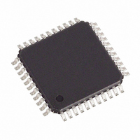
IC MCU FLASH 16KB 25MHZ 44-TQFP
Manufacturer
Maxim Integrated Products
Series
89Cr
Datasheet
1.DS89C450-KIT.pdf
(46 pages)
Specifications of DS89C430-ENG
Core Processor
8051
Core Size
8-Bit
Speed
25MHz
Connectivity
EBI/EMI, SIO, UART/USART
Peripherals
Power-Fail Reset, WDT
Number Of I /o
32
Program Memory Size
16KB (16K x 8)
Program Memory Type
FLASH
Ram Size
1K x 8
Voltage - Supply (vcc/vdd)
4.5 V ~ 5.5 V
Oscillator Type
External
Operating Temperature
-40°C ~ 85°C
Package / Case
44-TQFP, 44-VQFP
Processor Series
DS89C430
Core
8051
Data Bus Width
8 bit
Data Ram Size
1 KB
Interface Type
UART
Maximum Clock Frequency
33 MHz
Number Of Programmable I/os
4
Number Of Timers
3
Operating Supply Voltage
4.5 V to 5.5 V
Maximum Operating Temperature
+ 85 C
Mounting Style
SMD/SMT
3rd Party Development Tools
PK51, CA51, A51, ULINK2
Minimum Operating Temperature
- 40 C
Lead Free Status / RoHS Status
Contains lead / RoHS non-compliant
Eeprom Size
-
Data Converters
-
Available stocks
Company
Part Number
Manufacturer
Quantity
Price
Company:

Part Number:
DS89C430-ENG
Manufacturer:
Maxim Integrated
Quantity:
10 000
Company:
Part Number:
DS89C430-ENG+
Manufacturer:
Maxim Integrated
Quantity:
10 000


PIN DESCRIPTION
PDIP
40
20
19
18
29
30
39
38
37
36
35
34
33
32
9
1, 22, 23,
PLCC
12, 44
34
10
21
20
32
33
43
42
41
40
39
38
37
36
PIN
16, 17, 28,
TQFP
6, 38
39
15
14
26
27
37
36
35
34
33
32
31
30
4
ALE/PROG
P0.0 (AD0)
P0.1 (AD1)
P0.2 (AD2)
P0.3 (AD3)
P0.4 (AD4)
P0.5 (AD5)
P0.6 (AD6)
P0.7 (AD7)
NAME
XTAL1
XTAL2
PSEN
GND
RST
V
CC
+5V
Logic Ground
External Reset. The RST input pin is bidirectional and contains a Schmitt Trigger to
recognize external active-high reset inputs. The pin also employs an internal pulldown
resistor to allow for a combination of wire-ORed external reset sources. An RC is not
required for power-up, as the device provides this function internally.
Crystal Oscillators. These pins provide support for fundamental-mode parallel-resonant
AT-cut crystals. XTAL1 also acts as an input if there is an external clock source in place of
a crystal. XTAL2 serves as the output of the crystal amplifier.
Program Store Enable. This signal is commonly connected to optional external program
memory as a chip enable. PSEN provides an active-low pulse and is driven high when
external program memory is not being accessed. In one-cycle page mode 1, PSEN
remains low for consecutive page hits.
Address Latch Enable. This signal functions as a clock to latch the external address LSB
from the multiplexed address/data bus on Port 0. This signal is commonly connected to the
latch enable of an external 373-family transparent latch. In default mode, ALE has a pulse
width of 1.5 XTAL1 cycles and a period of four XTAL1 cycles. In page mode, the ALE
pulse width is altered according to the page mode selection. In traditional 8051 mode, ALE
is high when using the EMI reduction mode and during a reset condition. ALE can be
enabled by writing ALEON = 1 (PMR.2). Note that ALE operates independently of ALEON
during external memory accesses. As an alternate mode, this pin (PROG) is used to
execute the parallel program function.
Port 0 (AD0–AD7), I/O. Port 0 is an open-drain, 8-bit, bidirectional I/O port. As an
alternate function, Port 0 can function as the multiplexed address/data bus to access off-
chip memory. During the time when ALE is high, the LSB of a memory address is
presented. When ALE falls to logic 0, the port transitions to a bidirectional data bus. This
bus is used to read external program memory and read/write external RAM or peripherals.
When used as a memory bus, the port provides weak pullups for logic 1 outputs. The reset
condition of port 0 is tri-state. Pullup resistors are required only when using port 0 as an
I/O port.
DS89C430/DS89C450 Ultra-High-Speed Flash Microcontrollers
12 of 46
FUNCTION
Related parts for DS89C430-ENG
Image
Part Number
Description
Manufacturer
Datasheet
Request
R

Part Number:
Description:
IC MCU FLASH 16KB 25MHZ 44-TQFP
Manufacturer:
Maxim Integrated Products
Datasheet:
Part Number:
Description:
IC MCU FLASH 16KB 33MHZ 44-TQFP
Manufacturer:
Maxim Integrated Products
Datasheet:

Part Number:
Description:
IC MCU FLASH 16KB 25MHZ 44-PLCC
Manufacturer:
Maxim Integrated Products
Datasheet:

Part Number:
Description:
IC MCU FLASH 16KB 33MHZ 40-DIP
Manufacturer:
Maxim Integrated Products
Datasheet:
Part Number:
Description:
IC MCU FLASH 16KB 33MHZ 44-PLCC
Manufacturer:
Maxim Integrated Products
Datasheet:
Part Number:
Description:
IC MCU FLASH 16KB 25MHZ 40-DIP
Manufacturer:
Maxim Integrated Products
Datasheet:
Part Number:
Description:
IC MCU FLASH 16KB 33MHZ 44-TQFP
Manufacturer:
Maxim Integrated Products
Datasheet:
Part Number:
Description:
IC MCU FLASH 16KB 25MHZ 44-PLCC
Manufacturer:
Maxim Integrated Products
Datasheet:
Part Number:
Description:
IC MCU FLASH 16KB 25MHZ 40-DIP
Manufacturer:
Maxim Integrated Products
Datasheet:
Part Number:
Description:
IC MCU FLASH 16KB 33MHZ 44-PLCC
Manufacturer:
Maxim Integrated Products
Datasheet:
Part Number:
Description:
IC MCU FLASH 16KB 33MHZ 40-DIP
Manufacturer:
Maxim Integrated Products
Datasheet:

Part Number:
Description:
MAX7528KCWPMaxim Integrated Products [CMOS Dual 8-Bit Buffered Multiplying DACs]
Manufacturer:
Maxim Integrated Products
Datasheet:
Part Number:
Description:
Single +5V, fully integrated, 1.25Gbps laser diode driver.
Manufacturer:
Maxim Integrated Products
Datasheet:
Part Number:
Description:
Single +5V, fully integrated, 155Mbps laser diode driver.
Manufacturer:
Maxim Integrated Products
Datasheet:
Part Number:
Description:
VRD11/VRD10, K8 Rev F 2/3/4-Phase PWM Controllers with Integrated Dual MOSFET Drivers
Manufacturer:
Maxim Integrated Products
Datasheet: