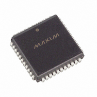
DS89C430-QNL Maxim Integrated Products, DS89C430-QNL Datasheet - Page 29

DS89C430-QNL
Manufacturer Part Number
DS89C430-QNL
Description
IC MCU FLASH 16KB 33MHZ 44-PLCC
Manufacturer
Maxim Integrated Products
Series
89Cr
Datasheet
1.DS89C450-KIT.pdf
(46 pages)
Specifications of DS89C430-QNL
Core Processor
8051
Core Size
8-Bit
Speed
33MHz
Connectivity
EBI/EMI, SIO, UART/USART
Peripherals
Power-Fail Reset, WDT
Number Of I /o
32
Program Memory Size
16KB (16K x 8)
Program Memory Type
FLASH
Ram Size
1K x 8
Voltage - Supply (vcc/vdd)
4.5 V ~ 5.5 V
Oscillator Type
External
Operating Temperature
-40°C ~ 85°C
Package / Case
44-LCC, 44-PLCC
Processor Series
DS89C430
Core
8051
Data Bus Width
8 bit
Data Ram Size
1 KB
Interface Type
UART
Maximum Clock Frequency
33 MHz
Number Of Programmable I/os
4
Number Of Timers
3
Operating Supply Voltage
4.5 V to 5.5 V
Maximum Operating Temperature
+ 85 C
Mounting Style
SMD/SMT
3rd Party Development Tools
PK51, CA51, A51, ULINK2
Minimum Operating Temperature
- 40 C
Lead Free Status / RoHS Status
Contains lead / RoHS non-compliant
Eeprom Size
-
Data Converters
-
Available stocks
Company
Part Number
Manufacturer
Quantity
Price
Company:
Part Number:
DS89C430-QNL
Manufacturer:
Maxim Integrated
Quantity:
10 000
Part Number:
DS89C430-QNL
Manufacturer:
MAXIM/美信
Quantity:
20 000
Company:
Part Number:
DS89C430-QNL+
Manufacturer:
DALLAS
Quantity:
12 000
Company:
Part Number:
DS89C430-QNL+
Manufacturer:
Maxim Integrated
Quantity:
10 000
Page Mode, External Memory Cycle
Page mode retains the basic circuitry requirement for an original 8051 external memory interface, but alters the
configuration of P0 and P2 for the purposes of address output and data I/O during external memory cycles.
Additionally, the functions of ALE and PSEN are altered to support this mode of operation.
Setting the PAGEE (ACON.7) bit to logic 1 enables page mode. Clearing the PAGEE bit to logic 0 disables the
page mode and the external bus structure defaults to the original 8051 expanded bus configuration (nonpage
mode). The DS89C430 supports page mode in two external bus structures. The logic value of the page-mode-
select bits in the ACON register determines the external bus structure and the basic memory cycle in number of
system clocks.
different memory cycle time. Setting the select bits to 11b selects another bus structure. Write access to the ACON
register requires a timed access.
Table 6. Page Mode Select
The first page mode’s (page mode 1) external bus structure uses P2 as the primary address bus, (multiplexing both
the most significant byte and least significant byte of the address for each external memory cycle) and P0 is used
as the primary data bus. During external code fetches, P0 is held in a high-impedance state by the processor. Op
codes are driven by the external memory onto P0 and latched at the end of the external fetch cycle at the rising
edge of PSEN. During external data read/write operations, P0 functions as the data I/O bus. It is held in a high-
impedance state for external reads from data memory and driven with data during external writes to data memory.
address. The external memory machine cycle can be 2, 4, or 8 system clocks in length for a page miss.
address. The external memory machine cycle can be 1, 2, or 4 system clocks in length for a page hit.
During a page hit, P2 drives Addr [0–7] of the 16-bit address, while the most significant address byte is held in the
external address latches. PSEN, RD, and WR strobes accordingly for the appropriate operation on the P0 data bus.
There is no ALE assertion for page hits.
PAGES1:PAGES0
A page miss occurs when the most significant byte of the subsequent address is different from the last
A page hit occurs when the most significant byte of the subsequent address does not change from the last
00
01
10
11
Table 6
CLOCKS PER MEMORY CYCLE
summarizes this option. The first three selections use the same bus structure but with
PAGE-HIT
1
2
4
2
PAGE-MISS
2
4
8
4
DS89C430/DS89C450 Ultra-High-Speed Flash Microcontrollers
29 of 46
P0: Primary data bus.
P2: Primary address bus, multiplexing both the upper byte and
lower byte of address.
P0: Primary data bus.
P2: Primary address bus, multiplexing both the upper byte and
lower byte of address.
P0: Primary data bus.
P2: Primary address bus, multiplexing both the upper byte and
lower byte of address.
P0: Lower address byte.
P2: The upper address byte is multiplexed with the data byte.
Note: This setting affects external code fetches only; accessing
the external data memory requires four clock cycles, regardless
of page hit or miss.
EXTERNAL BUS STRUCTURE


