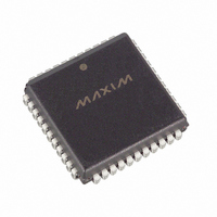
DS89C450-QNG+ Maxim Integrated Products, DS89C450-QNG+ Datasheet - Page 33

DS89C450-QNG+
Manufacturer Part Number
DS89C450-QNG+
Description
IC MCU FLASH 64KB 25MHZ 44-PLCC
Manufacturer
Maxim Integrated Products
Series
89Cr
Datasheet
1.DS89C450-KIT.pdf
(46 pages)
Specifications of DS89C450-QNG+
Core Processor
8051
Core Size
8-Bit
Speed
25MHz
Connectivity
EBI/EMI, SIO, UART/USART
Peripherals
Power-Fail Reset, WDT
Number Of I /o
32
Program Memory Size
64KB (64K x 8)
Program Memory Type
FLASH
Ram Size
1K x 8
Voltage - Supply (vcc/vdd)
4.5 V ~ 5.5 V
Oscillator Type
External
Operating Temperature
-40°C ~ 85°C
Package / Case
44-LCC, 44-PLCC
Processor Series
DS89C450
Core
8051
Data Bus Width
8 bit
Data Ram Size
1 KB
Interface Type
UART
Maximum Clock Frequency
33 MHz
Number Of Programmable I/os
4
Number Of Timers
3
Operating Supply Voltage
4.5 V to 5.5 V
Maximum Operating Temperature
+ 85 C
Mounting Style
SMD/SMT
3rd Party Development Tools
PK51, CA51, A51, ULINK2
Development Tools By Supplier
DS89C450-KIT#
Minimum Operating Temperature
- 40 C
Lead Free Status / RoHS Status
Lead free / RoHS Compliant
Eeprom Size
-
Data Converters
-
Lead Free Status / Rohs Status
Details
Table 10. Page Mode 2, Data Memory Cycle Stretch Values (PAGES1:PAGES0 = 11)
As shown in the previous tables, the stretch feature supports eight stretched external data-memory access options,
which can be categorized into three timing groups. When the stretch value is cleared to 000b, there is no stretch on
external data memory access, and a MOVX instruction is completed in two basic memory cycles. When the stretch
value is set to 1, 2, or 3, the external data memory access is extended by 1, 2, or 3 stretch memory cycles,
respectively. Note that the first stretch value does not result in adding four system clocks to the control signals. This
is because the first stretch uses one system clock to create additional address setup and data bus float time and
one system clock to create additional address and data hold time. When using very slow RAM and peripherals, a
larger stretch value (4–7) can be selected. In this stretch category, two stretch cycles are used to create additional
setup (the ALE pulse width is also stretched by one stretch cycle for page miss) and one stretch cycle is used to
create additional hold time. The following timing diagrams illustrate the external data memory access at divide-by-1
system clock mode (CD1:CD0 = 10b).
Figure 12
PAGES1:PAGES0 = 01. The stretch cycle shown is for a stretch value of 1 and is coincident with a page miss.
Note that the first stretch value does not result in adding four system clocks to the RD/WR control signals. This is
because the first stretch uses one system clock to create additional setup and one system clock to create
additional hold time.
Figure 13
memory cycle is shorter than a page miss data memory cycle. The ALE pulse width is also stretched by a stretch
cycle in the case of a page miss.
The stretched data memory bus cycle timing relationship for PAGES = 11 is identical to nonpage mode operation
since the basic data memory cycle always contains four system clocks in this page mode operation.
MD2:MD0
000
001
010
011
100
101
110
111
shows the timing relationship for a slow peripheral interface (stretch value = 4). Note that a page hit data
illustrates the external data-memory stretch-cycle timing relationship when PAGEE = 1 and
STRETCH
CYCLES
10
0
1
2
3
7
8
9
4X/ 2X , CD1,
CD0 = 100
0.5
RD/WR PULSE WIDTH (IN NUMBER OF OSCILLATOR CLOCKS)
1
2
3
4
5
6
7
DS89C430/DS89C450 Ultra-High-Speed Flash Microcontrollers
4X/ 2X , CD1,
CD0 = 000
33 of 46
10
12
14
1
2
4
6
8
4X/ 2X , CD1,
CD0 = X10
12
16
20
24
28
2
4
8
4X/ 2X , CD1,
CD0 = X11
12,288
16,384
20,480
24,576
28,672
2048
4096
8192


