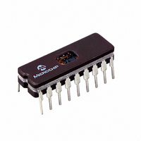
PIC16C715/JW Microchip Technology, PIC16C715/JW Datasheet - Page 37

PIC16C715/JW
Manufacturer Part Number
PIC16C715/JW
Description
IC MCU EPROM 2KX14 A/D 18CDIP
Manufacturer
Microchip Technology
Series
PIC® 16Cr
Specifications of PIC16C715/JW
Core Processor
PIC
Core Size
8-Bit
Speed
20MHz
Peripherals
Brown-out Detect/Reset, POR, WDT
Number Of I /o
13
Program Memory Size
3.5KB (2K x 14)
Program Memory Type
EPROM, UV
Ram Size
128 x 8
Voltage - Supply (vcc/vdd)
4 V ~ 5.5 V
Data Converters
A/D 4x8b
Oscillator Type
External
Operating Temperature
0°C ~ 70°C
Package / Case
18-CDIP (0.300", 7.62mm) Window
Lead Free Status / RoHS Status
Contains lead / RoHS non-compliant
Eeprom Size
-
Connectivity
-
Available stocks
Company
Part Number
Manufacturer
Quantity
Price
- Current page: 37 of 177
- Download datasheet (2Mb)
7.0
The analog-to-digital (A/D) converter module has four
analog inputs.
The A/D allows conversion of an analog input signal to
a corresponding 8-bit digital number (refer to Applica-
tion Note AN546 for use of A/D Converter). The output
of the sample and hold is the input into the converter,
which generates the result via successive approxima-
tion. The analog reference voltage is software select-
able to either the device’s positive supply voltage (V
or the voltage level on the RA3/AN3/V
FIGURE 7-1:
Applicable Devices
1997 Microchip Technology Inc.
bit7
bit 7-6: ADCS1:ADCS0: A/D Conversion Clock Select bits
bit 5:
bit 4-3: CHS1:CHS0: Analog Channel Select bits
bit 2:
bit 1:
bit 0:
ADCS1 ADCS0
Note 1: Bit5 of ADCON0 is a General Purpose R/W bit for the PIC16C710/711 only. For the PIC16C71, this bit is
R/W-0
ANALOG-TO-DIGITAL
CONVERTER (A/D) MODULE
00 = F
01 = F
10 = F
11 = F
Unimplemented: Read as '0'.
00 = channel 0, (RA0/AN0)
01 = channel 1, (RA1/AN1)
10 = channel 2, (RA2/AN2)
11 = channel 3, (RA3/AN3)
GO/DONE: A/D Conversion Status bit
If ADON = 1:
1 = A/D conversion in progress (setting this bit starts the A/D conversion)
0 = A/D conversion not in progress (This bit is automatically cleared by hardware when the A/D conver-
sion is complete)
ADIF: A/D Conversion Complete Interrupt Flag bit
1 = conversion is complete (must be cleared in software)
0 = conversion is not complete
ADON: A/D On bit
1 = A/D converter module is operating
0 = A/D converter module is shutoff and consumes no operating current
unimplemented, read as '0'.
R/W-0
ADCON0 REGISTER (ADDRESS 08h), PIC16C710/71/711
OSC
OSC
OSC
RC
(clock derived from an RC oscillation)
/2
/8
/32
—
U-0
710 71 711 715
(1)
R/W-0
CHS1
REF
pin.
R/W-0
CHS0
DD
)
GO/DONE
R/W-0
The A/D converter has a unique feature of being able
to operate while the device is in SLEEP mode. To oper-
ate in sleep, the A/D conversion clock must be derived
from the A/D’s internal RC oscillator.
The A/D module has three registers. These registers
are:
The ADCON0 register, shown in Figure 7-1 and
Figure 7-2, controls the operation of the A/D module.
The ADCON1 register, shown in Figure 7-3 configures
the functions of the port pins. The port pins can be con-
figured as analog inputs (RA3 can also be a voltage ref-
erence) or as digital I/O.
• A/D Result Register (ADRES)
• A/D Control Register 0 (ADCON0)
• A/D Control Register 1 (ADCON1)
R/W-0
ADIF
ADON
R/W-0
bit0
PIC16C71X
R = Readable bit
W = Writable bit
U = Unimplemented
- n =Value at POR reset
bit, read as ‘0’
DS30272A-page 37
Related parts for PIC16C715/JW
Image
Part Number
Description
Manufacturer
Datasheet
Request
R

Part Number:
Description:
IC MCU EPROM 1KX14 A/D 18CDIP
Manufacturer:
Microchip Technology
Datasheet:

Part Number:
Description:
IC MCU OTP 1KX14 A/D 18DIP
Manufacturer:
Microchip Technology
Datasheet:

Part Number:
Description:
IC MCU OTP 1KX14 A/D 18SOIC
Manufacturer:
Microchip Technology
Datasheet:

Part Number:
Description:
IC MCU OTP 1KX14 A/D 18DIP
Manufacturer:
Microchip Technology
Datasheet:

Part Number:
Description:
IC MCU OTP 1KX14 A/D 18DIP
Manufacturer:
Microchip Technology
Datasheet:

Part Number:
Description:
IC MCU OTP 1KX14 A/D 18SOIC
Manufacturer:
Microchip Technology
Datasheet:

Part Number:
Description:
IC MCU OTP 1KX14 A/D 18SOIC
Manufacturer:
Microchip Technology
Datasheet:

Part Number:
Description:
IC MCU OTP 1KX14 A/D 18SOIC
Manufacturer:
Microchip Technology
Datasheet:

Part Number:
Description:
IC MCU OTP 1KX14 A/D 18DIP
Manufacturer:
Microchip Technology
Datasheet:

Part Number:
Description:
8-Bit CMOS Microcontrollers with A/D Converter
Manufacturer:
Microchip Technology
Datasheet:

Part Number:
Description:
8-Bit CMOS Microcontrollers with A/D Converter
Manufacturer:
Microchip Technology

Part Number:
Description:
8-Bit CMOS Microcontrollers with A/D Converter
Manufacturer:
Microchip Technology

Part Number:
Description:
8-Bit CMOS Microcontrollers with A/D Converter
Manufacturer:
Microchip Technology

Part Number:
Description:
8-Bit CMOS Microcontrollers with A/D Converter
Manufacturer:
Microchip Technology

Part Number:
Description:
8-Bit CMOS Microcontrollers with A/D Converter
Manufacturer:
Microchip Technology


