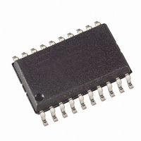
AT90S2313-4SC Atmel, AT90S2313-4SC Datasheet - Page 63

AT90S2313-4SC
Manufacturer Part Number
AT90S2313-4SC
Description
MCU 2K FLASH 4MHZ 20-SOIC
Manufacturer
Atmel
Series
AVR® 90Sr
Datasheet
1.AT90S2313-10PC.pdf
(92 pages)
Specifications of AT90S2313-4SC
Core Processor
AVR
Core Size
8-Bit
Speed
4MHz
Connectivity
SPI, UART/USART
Peripherals
Brown-out Detect/Reset, POR, PWM, WDT
Number Of I /o
15
Program Memory Size
2KB (1K x 16)
Program Memory Type
FLASH
Eeprom Size
128 x 8
Ram Size
128 x 8
Voltage - Supply (vcc/vdd)
2.7 V ~ 6 V
Oscillator Type
External
Operating Temperature
0°C ~ 70°C
Package / Case
20-SOIC (7.5mm Width)
Data Bus Width
8 bit
Data Ram Size
128 B
Interface Type
SPI, UART
Maximum Clock Frequency
4 MHz
Number Of Programmable I/os
15
Number Of Timers
1 x 8 bit
Operating Supply Voltage
2.7 V to 6 V
Maximum Operating Temperature
+ 70 C
Mounting Style
SMD/SMT
Minimum Operating Temperature
0 C
Lead Free Status / RoHS Status
Contains lead / RoHS non-compliant
Data Converters
-
Lead Free Status / Rohs Status
No
Available stocks
Company
Part Number
Manufacturer
Quantity
Price
Part Number:
AT90S2313-4SC
Manufacturer:
ATMEL/爱特梅尔
Quantity:
20 000
Programming the Flash
0839I–AVR–06/02
5. Give WR a
A: Load Command “Write Flash”
1. Set XA1, XA0 to “10”. This enables command loading.
2. Set BS to “0”.
3. Set DATA to “0001 0000”. This is the command for Write Flash.
4. Give XTAL1 a positive pulse. This loads the command.
B: Load Address High Byte
1. Set XA1, XA0 to “00”. This enables address loading.
2. Set BS to “1”. This selects high byte.
3. Set DATA = Address high byte ($00 - $03).
4. Give XTAL1 a positive pulse. This loads the address high byte.
C: Load Address Low Byte
1. Set XA1, XA0 to “00”. This enables address loading.
2. Set BS to “0”. This selects low byte.
3. Set DATA = Address low byte ($00 - $FF).
4. Give XTAL1 a positive pulse. This loads the address low byte.
D: Load Data Low Byte
1. Set XA1, XA0 to “01”. This enables data loading.
2. Set DATA = Data low byte ($00 - $FF).
3. Give XTAL1 a positive pulse. This loads the data low byte.
E: Write Data Low Byte
1. Set BS to “0”. This selects low data.
2. Give WR a negative pulse. This starts programming of the data byte. RDY/BSY
3. Wait until RDY/BSY goes high to program the next byte.
(See Figure 50 for signal waveforms.)
F: Load Data High Byte
1. Set XA1, XA0 to “01”. This enables data loading.
2. Set DATA = Data high byte ($00 - $FF).
3. Give XTAL1 a positive pulse. This loads the data high byte.
G: Write Data High Byte
1. Set BS to “1”. This selects high data.
2. Give WR a negative pulse. This starts programming of the data byte. RDY/BSY
3. Wait until RDY/BSY goes high to program the next byte.
(See Figure 51 for signal waveforms.)
for
pin.
goes low.
goes low.
t
WLWH_CE
t
WLWH_CE
value. Chip Erase does not generate any activity on the RDY/BSY
wide negative pulse to execute Chip Erase. See Table 26
AT90S2313
63


