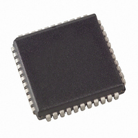
AT90S8515-4JC Atmel, AT90S8515-4JC Datasheet - Page 39

AT90S8515-4JC
Manufacturer Part Number
AT90S8515-4JC
Description
IC MCU 8K FLSH 4MHZ LV 44PLCC
Manufacturer
Atmel
Series
AVR® 90Sr
Datasheets
1.AT90S8515-4AC.pdf
(112 pages)
2.AT90S8515-4AC.pdf
(4 pages)
3.AT90S8515-4AC.pdf
(4 pages)
Specifications of AT90S8515-4JC
Core Processor
AVR
Core Size
8-Bit
Speed
4MHz
Connectivity
SPI, UART/USART
Peripherals
Brown-out Detect/Reset, POR, PWM, WDT
Number Of I /o
32
Program Memory Size
8KB (4K x 16)
Program Memory Type
FLASH
Eeprom Size
512 x 8
Ram Size
512 x 8
Voltage - Supply (vcc/vdd)
2.7 V ~ 6 V
Oscillator Type
Internal
Operating Temperature
0°C ~ 70°C
Package / Case
44-PLCC
Lead Free Status / RoHS Status
Contains lead / RoHS non-compliant
Data Converters
-
Timer/Counter1 Output
Compare Register – OCR1BH
AND OCR1BL
Timer/Counter1 Input Capture
Register – ICR1H AND ICR1L
0841G–09/01
The output compare registers are 16-bit read/write registers.
The Timer/Counter1 Output Compare registers contain the data to be continuously com-
pared with Timer/Counter1. Actions on compare matches are specified in the
Timer/Counter1 Control and Status registers. A compare match only occurs if
Timer/Counter1 counts to the OCR value. A software write that sets TCNT1 and OCR1A
or OCR1B to the same value does not generate a compare match.
A compare match will set the compare interrupt flag in the CPU clock cycle following the
compare event.
Since the Output Compare Registers (OCR1A and OCR1B) are 16-bit registers, a tem-
porary register (TEMP) is used when OCR1A/B are written to ensure that both bytes are
updated simultaneously. When the CPU writes the high byte, OCR1AH or OCR1BH, the
data is temporarily stored in the TEMP register. When the CPU writes the low byte,
OCR1AL or OCR1BL, the TEMP register is simultaneously written to OCR1AH or
OCR1BH. Consequently, the high byte OCR1AH or OCR1BH must be written first for a
full 16-bit register write operation.
The TEMP register is also used when accessing TCNT1 and ICR1. If the main program
and interrupt routines perform access to registers using TEMP, interrupts must be dis-
abled during access from the main program (and from interrupt routines if interrupts are
allowed from within interrupt routines).
The input capture register is a 16-bit read-only register.
When the rising or falling edge (according to the input capture edge setting [ICES1]) of
the signal at the input capture pin (ICP) is detected, the current value of the
Timer/Counter1 is transferred to the Input Capture Register (ICR1). At the same time,
the input capture flag (ICF1) is set (one).
Since the Input Capture Register (ICR1) is a 16-bit register, a temporary register
(TEMP) is used when ICR1 is read to ensure that both bytes are read simultaneously.
When the CPU reads the low byte ICR1L, the data is sent to the CPU and the data of
the high byte ICR1H is placed in the TEMP register. When the CPU reads the data in
the high byte ICR1H, the CPU receives the data in the TEMP register. Consequently,
the low byte ICR1L must be accessed first for a full 16-bit register read operation.
Bit
$29 ($49)
$28 ($48)
Read/Write
Initial Value
Bit
$25 ($45)
$24 ($44)
Read/Write
Initial Value
MSB
MSB
R/W
R/W
15
15
R
R
7
0
0
7
0
0
R/W
R/W
14
14
R
R
6
0
0
6
0
0
R/W
R/W
13
13
R
R
5
0
0
5
0
0
R/W
R/W
12
12
4
0
0
4
R
R
0
0
R/W
R/W
11
11
R
R
3
0
0
3
0
0
R/W
R/W
10
10
R
R
2
0
0
2
0
0
R/W
R/W
R
R
9
0
9
0
1
0
1
0
AT90S8515
LSB
R/W
LSB
R/W
R
R
8
0
0
0
8
0
0
0
OCR1BH
OCR1BL
ICR1H
ICR1L
39


