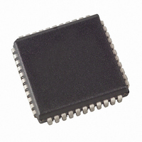
AT89S53-24JI Atmel, AT89S53-24JI Datasheet - Page 7

AT89S53-24JI
Manufacturer Part Number
AT89S53-24JI
Description
MICRO CONTROLLER
Manufacturer
Atmel
Series
89Sr
Datasheet
1.AT89S53-24JI.pdf
(35 pages)
Specifications of AT89S53-24JI
Core Processor
8051
Core Size
8-Bit
Speed
24MHz
Connectivity
SPI, UART/USART
Peripherals
WDT
Number Of I /o
32
Program Memory Size
12KB (12K x 8)
Program Memory Type
FLASH
Ram Size
256 x 8
Voltage - Supply (vcc/vdd)
4 V ~ 6 V
Oscillator Type
Internal
Operating Temperature
-40°C ~ 85°C
Package / Case
44-PLCC
Data Bus Width
8 bit
Data Ram Size
256 B
Interface Type
SPI, UART
Maximum Clock Frequency
24 MHz
Number Of Programmable I/os
32
Number Of Timers
3 x 16 bit
Operating Supply Voltage
4 V to 6 V
Maximum Operating Temperature
+ 85 C
Mounting Style
SMD/SMT
Minimum Operating Temperature
- 40 C
Lead Free Status / RoHS Status
Contains lead / RoHS non-compliant
Eeprom Size
-
Data Converters
-
Lead Free Status / Rohs Status
No
Other names
Q1036833
Available stocks
Company
Part Number
Manufacturer
Quantity
Price
Company:
Part Number:
AT89S53-24JI
Manufacturer:
ATM
Quantity:
620
Company:
Part Number:
AT89S53-24JI
Manufacturer:
ATM
Quantity:
620
Part Number:
AT89S53-24JI
Manufacturer:
ATMEL/爱特梅尔
Quantity:
20 000
Table 3. WCON—Watchdog Control Register
SPI Registers Control and status bits for the Serial Periph-
eral Interface are contained in registers SPCR (shown in
Table 4) and SPSR (shown in Table 5). The SPI data bits
are contained in the SPDR register. Writing the SPI data
register during serial data transfer sets the Write Collision
bit, WCOL, in the SPSR register. The SPDR is double buff-
ered for writing and the values in SPDR are not changed by
Reset.
Interrupt Registers The global interrupt enable bit and the
individual interrupt enable bits are in the IE register. In
addition, the individual interrupt enable bit for the SPI is in
the SPCR register. Two priorities can be set for each of the
six interrupt sources in the IP register.
0787E–MICRO–3/06
WCON Address = 96H
Symbol
PS2
PS1
PS0
DPS
WDTRST
WDTEN
Bit
PS2
7
Function
Prescaler Bits for the Watchdog Timer. When all three bits are set to “0”, the watchdog timer has a nominal period of 16
ms. When all three bits are set to “1”, the nominal period is 2048 ms.
Data Pointer Register Select. DPS = 0 selects the first bank of Data Pointer Register, DP0, and DPS = 1 selects the
second bank, DP1
Watchdog Timer Reset. Each time this bit is set to “1” by user software, a pulse is generated to reset the watchdog
timer. The WDTRST bit is then automatically reset to “0” in the next instruction cycle. The WDTRST bit is Write-Only.
Watchdog Timer Enable Bit. WDTEN = 1 enables the watchdog timer and WDTEN = 0 disables the watchdog timer.
PS1
6
PS0
5
reserved
4
Dual Data Pointer Registers To facilitate accessing exter-
nal data memory, two banks of 16-bit Data Pointer
Registers are provided: DP0 at SFR address locations
82H-83H and DP1 at 84H-85H. Bit DPS = 0 in SFR WCON
selects DP0 and DPS = 1 selects DP1. The user should
always initalize the DPS bit to the appropriate value before
accessing the respective Data Pointer register.
Power Off Flag The Power Off Flag (POF) is located at
bit_4 (PCON.4) in the PCON SFR. POF is set to “1” during
power up. It can be set and reset under software control
and is not affected by RESET.
reserved
3
DPS
2
Reset Value = 0000 0010B
WDTRST
1
AT89S53
WDTEN
0
7


