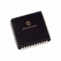
PIC18F442T-E/L Microchip Technology, PIC18F442T-E/L Datasheet

PIC18F442T-E/L
Specifications of PIC18F442T-E/L
Related parts for PIC18F442T-E/L
PIC18F442T-E/L Summary of contents
Page 1
... INTCON and PIE registers to their pre-instruction state. Date Codes that pertain to this issue: All engineering and production devices. © 2005 Microchip Technology Inc. PIC18FXX2 2. Module: Data EEPROM When reading the data EEPROM, the contents of the EEDATA register may become corrupted in the second instruction cycle after the RD bit (EECON1< ...
Page 2
... This is a recommended solution. Others may exist. Date Codes that pertain to this issue: All engineering samples and devices with date codes up to and including 0252 (Year 2002, Work Week 52). © 2005 Microchip Technology Inc. over ID locations bytes ...
Page 3
... Date Codes that pertain to this issue: All engineering samples and devices with date codes up to and including 0252 (Year 2002, Work Week 52). © 2005 Microchip Technology Inc. PIC18FXX2 7. Module: Data EEPROM When reading the data EEPROM, the contents of the EEDATA register may be corrupted if the RD bit (EECON1< ...
Page 4
... Affected systems will repeatably fail normal testing. Systems not affected will continue to not be affected over time. Work around Insert a NOP instruction at address 0x0000. Date Codes that pertain to this issue: All engineering and production devices. © 2005 Microchip Technology Inc. ...
Page 5
... Sleep mode, with all I/O pins in hi-impedance state and tied to V features that add delta current disabled (such as WDT, Timer1 Oscillator, BOR,...). 4: For RC osc configuration, current through R estimated by the formula © 2005 Microchip Technology Inc. Standard Operating Conditions (unless otherwise stated) -40°C ≤ T Operating temperature Standard Operating Conditions (unless otherwise stated) -40° ...
Page 6
... Device Data Sheet. “MLF” should be considered an obsoleted term PIC18F442 PIC18F452 Example PIC18F442 -I/ML OSC2/CLKO/RA6 OSC1/CLKI RE2/AN7/CS RE1/AN6/WR RE0/AN5/RD RA5/AN4/SS/LVDIN RA4/T0CKI 0510017 © 2005 Microchip Technology Inc. ...
Page 7
... RA5 AN4 SS LVDIN RA6 Legend: TTL = TTL compatible input ST = Schmitt Trigger input with CMOS levels O = Output OD = Open Drain (no P diode to V © 2005 Microchip Technology Inc. Pin Buffer Type Type 18 Master Clear (input) or high voltage ICSP™ programming enable pin Master Clear (Reset) input. This pin is an active low Reset to the device ...
Page 8
... I/O TTL Digital I/O. Interrupt-on-change pin. I/O ST In-Circuit Debugger and ICSP programming clock pin. 17 I/O TTL Digital I/O. Interrupt-on-change pin. I/O ST In-Circuit Debugger and ICSP programming data pin. CMOS = CMOS compatible input or output I = Input P = Power ) DD Description © 2005 Microchip Technology Inc. ...
Page 9
... TX CK RC7/RX/ RC7 RX DT Legend: TTL = TTL compatible input ST = Schmitt Trigger input with CMOS levels O = Output OD = Open Drain (no P diode to V © 2005 Microchip Technology Inc. Pin Buffer Type Type PORTC is a bidirectional I/O port. 32 I/O ST Digital I/O. O — Timer1 oscillator output. ...
Page 10
... Ground reference for logic and I/O pins — Positive supply for logic and I/O pins. 12, 13, — — These pins are not internally connected. They 33, 34 should be left unconnected. CMOS = CMOS compatible input or output I = Input P = Power ) DD Description © 2005 Microchip Technology Inc. ...
Page 11
... Parameter Notes: 1. BSC: Basic Dimension. Theoretically exact value shown without tolerances. See ASME Y14.5M 2. REF: Reference Dimension, usually without tolerance, for information purposes only. See ASME Y14.5M JEDEC equivalent: M0-220 Drawing No. C04-103 © 2005 Microchip Technology Inc. EXPOSED METAL PAD ...
Page 12
... Space). Added silicon issues 8, 9 and 10 (MSSP and Core - Instruction Set) and data sheet clarification 2 (Packaging - Pinout and Product Identification). Rev F Document (7/2003) Added silicon issue 11 (Timer1 Oscillator). Rev G Document (05/2005) Added silicon issue 12 (Reset). DS80127G-page 12 © 2005 Microchip Technology Inc. ...
Page 13
... PowerMate, PowerTool, rfLAB, rfPICDEM, Select Mode, Smart Serial, SmartTel, Total Endurance and WiperLock are trademarks of Microchip Technology Incorporated in the U.S.A. and other countries. SQTP is a service mark of Microchip Technology Incorporated in the U.S.A. All other trademarks mentioned herein are property of their respective companies. ...
Page 14
... Fax: 65-6334-8850 Taiwan - Kaohsiung Tel: 886-7-536-4818 Fax: 886-7-536-4803 Taiwan - Taipei Tel: 886-2-2500-6610 Fax: 886-2-2508-0102 Taiwan - Hsinchu Tel: 886-3-572-9526 Fax: 886-3-572-6459 © 2005 Microchip Technology Inc. EUROPE Austria - Weis Tel: 43-7242-2244-399 Fax: 43-7242-2244-393 Denmark - Ballerup Tel: 45-4450-2828 Fax: 45-4485-2829 France - Massy Tel: 33-1-69-53-63-20 ...


