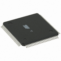
ATMEGA6450-16AI Atmel, ATMEGA6450-16AI Datasheet - Page 284

ATMEGA6450-16AI
Manufacturer Part Number
ATMEGA6450-16AI
Description
IC AVR MCU FLASH 64K 5V 100TQFP
Manufacturer
Atmel
Series
AVR® ATmegar
Datasheet
1.ATMEGA325-16MU.pdf
(362 pages)
Specifications of ATMEGA6450-16AI
Core Processor
AVR
Core Size
8-Bit
Speed
16MHz
Connectivity
SPI, UART/USART, USI
Peripherals
Brown-out Detect/Reset, POR, PWM, WDT
Number Of I /o
68
Program Memory Size
64KB (32K x 16)
Program Memory Type
FLASH
Eeprom Size
2K x 8
Ram Size
4K x 8
Voltage - Supply (vcc/vdd)
2.7 V ~ 5.5 V
Data Converters
A/D 8x10b
Oscillator Type
Internal
Operating Temperature
-40°C ~ 85°C
Package / Case
100-TQFP, 100-VQFP
For Use With
ATSTK600-TQFP100 - STK600 SOCKET/ADAPTER 100-TQFPATSTK504 - STARTER KIT AVR EXP MOD 100P LCD
Lead Free Status / RoHS Status
Contains lead / RoHS non-compliant
Available stocks
Company
Part Number
Manufacturer
Quantity
Price
- Current page: 284 of 362
- Download datasheet (7Mb)
Figure 26-12. Serial Programming Instruction example
26.7.4
26.8
2570M–AVR–04/11
Byte 1
Programming via the JTAG Interface
SPI Serial Programming Characteristics
Load Program Memory Page (High/Low Byte)/
Load EEPROM Memory Page (page access)
Bit 15 B
Byte 2
Adr M M S S B
A
For characteristics of the SPI module see “SPI Timing Characteristics” on page 302.
Programming through the JTAG interface requires control of the four JTAG specific pins: TCK,
TMS, TDI, and TDO. Control of the reset and clock pins is not required.
To be able to use the JTAG interface, the JTAGEN Fuse must be programmed. The device is
default shipped with the fuse programmed. In addition, the JTD bit in MCUCSR must be cleared.
Alternatively, if the JTD bit is set, the external reset can be forced low. Then, the JTD bit will be
cleared after two chip clocks, and the JTAG pins are available for programming. This provides a
means of using the JTAG pins as normal port pins in Running mode while still allowing In-Sys-
tem Programming via the JTAG interface. Note that this technique can not be used when using
the JTAG pins for Boundary-scan or On-chip Debug. In these cases the JTAG pins must be ded-
icated for this purpose.
During programming the clock frequency of the TCK Input must be less than the maximum fre-
quency of the chip. The System Clock Prescaler can not be used to divide the TCK Clock Input
into a sufficiently low frequency.
As a definition in this data sheet, the LSB is shifted in and out first of all Shift Registers.
Byte 3
Adr LSB
Page Offset
0
Serial Programming Instruction
Byte 4
Program Memory/
EEPROM Memory
Page Buffer
Page N-1
Page 0
Page 1
Page 2
Byte 1
ATmega325/3250/645/6450
Page Number
Bit 15 B
Byte 2
Write Program Memory Page/
Write EEPROM Memory Page
Adr MSB
Byte 3
A A dr r L L SB B
0
Byte 4
284
Related parts for ATMEGA6450-16AI
Image
Part Number
Description
Manufacturer
Datasheet
Request
R

Part Number:
Description:
Manufacturer:
Atmel Corporation
Datasheet:

Part Number:
Description:
IC AVR MCU FLASH 64K 64TQFP
Manufacturer:
Atmel
Datasheet:

Part Number:
Description:
IC AVR MCU FLASH 64K 5V 64TQFP
Manufacturer:
Atmel
Datasheet:

Part Number:
Description:
IC AVR MCU FLASH 64K 64-QFN
Manufacturer:
Atmel
Datasheet:

Part Number:
Description:
MCU AVR 64KB FLASH 16MHZ 64TQFP
Manufacturer:
Atmel
Datasheet:

Part Number:
Description:
MCU AVR 64KB FLASH 16MHZ 64QFN
Manufacturer:
Atmel
Datasheet:

Part Number:
Description:
IC AVR MCU FLASH 64K 5V 64QFN
Manufacturer:
Atmel
Datasheet:

Part Number:
Description:
Manufacturer:
Atmel Corporation
Datasheet:

Part Number:
Description:
Manufacturer:
ATMEL Corporation
Datasheet:

Part Number:
Description:
Manufacturer:
ATMEL Corporation
Datasheet:

Part Number:
Description:
IC AVR MCU 64K 16MHZ 5V 64TQFP
Manufacturer:
Atmel
Datasheet:

Part Number:
Description:
IC AVR MCU 64K 16MHZ 5V 64-QFN
Manufacturer:
Atmel
Datasheet:

Part Number:
Description:
IC AVR MCU 64K 16MHZ COM 64-TQFP
Manufacturer:
Atmel
Datasheet:

Part Number:
Description:
IC AVR MCU 64K 16MHZ IND 64-TQFP
Manufacturer:
Atmel
Datasheet:


