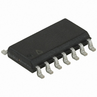
ATTINY44-20SSU Atmel, ATTINY44-20SSU Datasheet - Page 2

ATTINY44-20SSU
Manufacturer Part Number
ATTINY44-20SSU
Description
IC MCU AVR 4K FLASH 20MHZ 14SOIC
Manufacturer
Atmel
Series
AVR® ATtinyr
Specifications of ATTINY44-20SSU
Core Processor
AVR
Core Size
8-Bit
Speed
20MHz
Connectivity
USI
Peripherals
Brown-out Detect/Reset, POR, PWM, WDT
Number Of I /o
12
Program Memory Size
4KB (2K x 16)
Program Memory Type
FLASH
Eeprom Size
256 x 8
Ram Size
256 x 8
Voltage - Supply (vcc/vdd)
2.7 V ~ 5.5 V
Data Converters
A/D 8x10b
Oscillator Type
Internal
Operating Temperature
-40°C ~ 85°C
Package / Case
14-SOIC (3.9mm Width), 14-SOL
Cpu Family
ATtiny
Device Core
AVR
Device Core Size
8b
Frequency (max)
20MHz
Interface Type
SPI/USI
Total Internal Ram Size
256Byte
# I/os (max)
12
Number Of Timers - General Purpose
2
Operating Supply Voltage (typ)
3.3/5V
Operating Supply Voltage (max)
5.5V
Operating Supply Voltage (min)
2.7V
On-chip Adc
8-chx10-bit
Instruction Set Architecture
RISC
Operating Temp Range
-40C to 85C
Operating Temperature Classification
Industrial
Mounting
Surface Mount
Pin Count
14
Package Type
SOIC
For Use With
ATAVRISP2 - PROGRAMMER AVR IN SYSTEM
Lead Free Status / RoHS Status
Lead free / RoHS Compliant
- Current page: 2 of 238
- Download datasheet (5Mb)
1. Pin Configurations
Figure 1-1.
1.1
1.1.1
1.1.2
1.1.3
2
(PCINT6/OC1A/SDA/MOSI/DI/ADC6) PA6
(ADC4/USCK/SCL/T1/PCINT4) PA4
Pin Descriptions
ATtiny24/44/84
VCC
GND
Port B (PB3:PB0)
(PCINT10/INT0/OC0A/CKOUT) PB2
NOTE
Bottom pad should be
soldered to ground.
DNC: Do Not Connect
Pinout ATtiny24/44/84
(ADC0/AREF/PCINT0) PA0
(PCINT7/ICP/OC0B/ADC7) PA7
(ADC2/AIN1/PCINT2) PA2
(ADC1/AIN0/PCINT1) PA1
(ADC3/T0/PCINT3) PA3
(PCINT11/RESET/dW) PB3
(PCINT8/XTAL1/CLKI) PB0
(PCINT9/XTAL2) PB1
Supply voltage.
Ground.
Port B is a 4-bit bi-directional I/O port with internal pull-up resistors (selected for each bit). The
Port B output buffers have symmetrical drive characteristics with both high sink and source
capability except PB3 which has the RESET capability. To use pin PB3 as an I/O pin, instead of
RESET pin, program (‘0’) RSTDISBL fuse. As inputs, Port B pins that are externally pulled low
will source current if the pull-up resistors are activated. The Port B pins are tri-stated when a
reset condition becomes active, even if the clock is not running.
VCC
1
2
3
4
5
PDIP/SOIC
QFN/MLF
1
2
3
4
5
6
7
14
13
12
11
10
9
8
15
14
13
12
11
GND
PA0 (ADC0/AREF/PCINT0)
PA1 (ADC1/AIN0/PCINT1)
PA2 (ADC2/AIN1/PCINT2)
PA3 (ADC3/T0/PCINT3)
PA4 (ADC4/USCK/SCL/T1/PCINT4)
PA5 (ADC5/DO/MISO/OC1B/PCINT5)
Pin 16: PA6 (PCINT6/OC1A/SDA/MOSI/DI/ADC6)
Pin 20: PA5 (ADC5/DO/MISO/OC1B/PCINT5)
PA7 (PCINT7/ICP/OC0B/ADC7)
PB2 (PCINT10/INT0/OC0A/CKOUT)
PB3 (PCINT11/RESET/dW)
PB1 (PCINT9/XTAL2)
PB0 (PCINT8/XTAL1/CLKI)
8006K–AVR–10/10
Related parts for ATTINY44-20SSU
Image
Part Number
Description
Manufacturer
Datasheet
Request
R

Part Number:
Description:
Manufacturer:
Atmel Corporation
Datasheet:

Part Number:
Description:
Manufacturer:
Atmel Corporation
Datasheet:

Part Number:
Description:
MCU AVR 4K FLASH 15MHZ 20-QFN
Manufacturer:
Atmel
Datasheet:

Part Number:
Description:
IC MCU AVR 4K FLASH 20MHZ 20-QFN
Manufacturer:
Atmel
Datasheet:

Part Number:
Description:
MCU AVR 4KB FLASH 20MHZ 14SOIC
Manufacturer:
Atmel
Datasheet:

Part Number:
Description:
MCU AVR 4KB FLASH 20MHZ 20QFN
Manufacturer:
Atmel
Datasheet:

Part Number:
Description:
IC MCU AVR 4K FLASH 15MHZ 14SOIC
Manufacturer:
Atmel
Datasheet:

Part Number:
Description:
IC MCU AVR 4K FLASH 20MHZ 14-DIP
Manufacturer:
Atmel
Datasheet:

Part Number:
Description:
IC, MCU, 8BIT, 2K FLASH, 20SOIC
Manufacturer:
Atmel
Datasheet:

Part Number:
Description:
IC, MCU, 8BIT, 2K FLASH, 20PDIP
Manufacturer:
Atmel
Datasheet:

Part Number:
Description:
IC, MCU, 8BIT, 8K FLASH, 20PDIP
Manufacturer:
Atmel
Datasheet:

Part Number:
Description:
IC, MCU, 8BIT, 8K FLASH, 20SOIC
Manufacturer:
Atmel
Datasheet:

Part Number:
Description:
DEV KIT FOR AVR/AVR32
Manufacturer:
Atmel
Datasheet:


