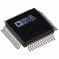
ADUC847BS32-3 Analog Devices Inc, ADUC847BS32-3 Datasheet - Page 27

ADUC847BS32-3
Manufacturer Part Number
ADUC847BS32-3
Description
IC FLASH MCU W/24BIT ADC 52-MQFP
Manufacturer
Analog Devices Inc
Series
MicroConverter® ADuC8xxr
Datasheet
1.EVAL-ADUC845QSZ.pdf
(108 pages)
Specifications of ADUC847BS32-3
Core Processor
8052
Core Size
8-Bit
Speed
12.58MHz
Connectivity
I²C, SPI, UART/USART
Peripherals
POR, PSM, PWM, Temp Sensor, WDT
Number Of I /o
34
Program Memory Size
32KB (32K x 8)
Program Memory Type
FLASH
Eeprom Size
4K x 8
Ram Size
2.25K x 8
Voltage - Supply (vcc/vdd)
2.7 V ~ 3.6 V
Data Converters
A/D 10x24b; D/A 1x12b, 2x16b
Oscillator Type
Internal
Operating Temperature
-40°C ~ 125°C
Package / Case
52-MQFP, 52-PQFP
For Use With
EVAL-ADUC847QSZ - KIT DEV QUICK START FOR ADUC847
Lead Free Status / RoHS Status
Contains lead / RoHS non-compliant
Signal Chain Overview (Chop Enabled, CHOP = 0)
With the CHOP bit = 0 (see the ADCMODE SFR bit designa-
tions in Table 24), the chopping scheme is enabled. This is the
default condition and gives optimum performance in terms of
offset errors and drift performance. With chop enabled, the
available output rates vary from 5.35 Hz to 105 Hz (SF = 255
and 13, respectively). A typical block diagram of the ADC input
channel with chop enabled is shown in Figure 12.
The sampling frequency of the modulator loop is many times
higher than the bandwidth of the input signal. The integrator in
the modulator shapes the quantization n
from the analog-to-digital conversion) so that the noise is pushe
toward one-half of the modulator frequency. The output of the
Σ-Δ modulator feeds directly into the digital filter. The digital
filter then band-limits the response to a frequency significantly
lower than one-half of the modulator frequency. In this manner,
the 1-bit output of the comparator is translated into a band
limited, low noise output from the ADCs.
The ADC filter is a low-pass Sinc
primary function is to remove the quantization noise introduced
at the modulator. The cutoff frequency and decimated output
data rate of the filter are programmable via the Sinc filter word
loaded into the filter (SF) register (see Table 28). The complete
signal chain is chopped, resulting in excellent dc offset and
offset drift specifications and is extremely beneficial in applica-
tions where drift, noise rejection, and optimum EMI rejection
are important.
ANALOG
INPUT
F
MUX
CHOP
3
or (sinx/x)
BUF
Figure 12. Block Diagram of the ADC Inpu
oise (which results
3
PGA
filter whose
F
IN
F
MOD
MOD
Σ-∆
Rev. B | Page 27 of 108
d
F
XOR
CHOP
With
deci
have
resu
word
filter
to th
factor is restricted to an 8-bit register called SF (see Table 28),
th
Therefore, the decimated output rate from the Sinc
the ADC conversion rate) is
where:
f
SF is the decimal equivalent of the word loaded to the filter
register.
f
The chop rate of the channel is half the output data rate:
As shown in the block diagram (Figure 12), the Sinc
outputs alternately contain +V
respective channel offset.
SINC
t Channel with Chop Enabled
ADC
MOD
e actual decimation factor is the register value times 8.
3
mated digital output words from the Sinc
lt, a final summing stage is included so that each output
is the ADC conversion rate.
is the modulator sampling rate of 32.768 kHz.
e ADC data register. Programming the Sinc
a positive offset and a negative offset term included. As a
FILTER
output to produce a new valid output result to be written
chop enabled, the ADC repeatedly reverses its inputs. The
from the filter is summed and averaged with the previous
f
f
CHOP
ADC
=
=
1
3
2
×
3 × (8 × SF)
×
8
f
×
1
ADC
1
SF
ADuC845/ADuC847/ADuC848
AIN + V
AIN – V
×
F
ADC
f
MOD
OS
OS
Σ-∆
OS
2
and −V
DIGITAL
OUTPUT
OS
, where V
3
filter, therefore,
3
decimation
3
OS
3
filter (and
filter
is the


