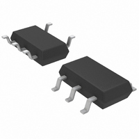
LT6220CS5#TRMPBF Linear Technology, LT6220CS5#TRMPBF Datasheet

LT6220CS5#TRMPBF
Specifications of LT6220CS5#TRMPBF
Available stocks
Related parts for LT6220CS5#TRMPBF
LT6220CS5#TRMPBF Summary of contents
Page 1
... SSOP package. The LT6220/ LT6221/ LT6222 can be used as plug-in replacements for many op amps to improve input/output range and performance. , LTC and LT are registered trademarks of Linear Technology Corporation. ThinSOT is a trademark of Linear Technology Corporation ...
Page 2
LT6220/LT6221/LT6222 ABSOLUTE AXI U RATI GS – + Total Supply Voltage ( ......................... 12. Input Voltage (Note 2) .............................................. ±V Input Current (Note 2) ........................................ ±10mA Output Short Circuit Duration (Note 3) ...
Page 3
ELECTRICAL CHARACTERISTICS T = 25° 5V, 0V 3V, 0V SYMBOL PARAMETER V Input Offset Voltage OS ∆V Input Offset Voltage Shift OS Input Offset Voltage Match (Channel-to-Channel) (Note 9) I Input ...
Page 4
LT6220/LT6221/LT6222 ELECTRICAL CHARACTERISTICS temperature range 5V, 0V 3V, 0V SYMBOL PARAMETER V Input Offset Voltage OS ∆V Input Offset Voltage Shift OS Input Offset Voltage Match (Channel-to-Channel) V (Note Input ...
Page 5
ELECTRICAL CHARACTERISTICS temperature range 5V, 0V 3V, 0V SYMBOL PARAMETER V Input Offset Voltage OS ∆V Input Offset Voltage Shift OS Input Offset Voltage Match (Channel-to-Channel) V (Note Input Offset ...
Page 6
LT6220/LT6221/LT6222 ELECTRICAL CHARACTERISTICS = ±5V 25° 0V 0V, unless otherwise noted OUT SYMBOL PARAMETER V Input Offset Voltage OS ∆V Input Offset Voltage Shift OS Input Offset Voltage Match (Channel-to-Channel) ...
Page 7
ELECTRICAL CHARACTERISTICS = ±5V, V temperature range 0V SYMBOL PARAMETER V Input Offset Voltage OS ∆V Input Offset Voltage Shift OS Input Offset Voltage Match (Channel-to-Channel) V (Note Input Offset Voltage Drift ...
Page 8
LT6220/LT6221/LT6222 ELECTRICAL CHARACTERISTICS = ±5V, V temperature range 0V SYMBOL PARAMETER V Input Offset Voltage OS ∆V Input Offset Voltage Shift OS Input Offset Voltage Match (Channel-to-Channel) V (Note Input Offset Voltage ...
Page 9
W U TYPICAL PERFOR A CE CHARACTERISTICS V Distribution (S8, PNP Stage 5V –250 –150 –50 ...
Page 10
LT6220/LT6221/LT6222 W U TYPICAL PERFOR A CE CHARACTERISTICS Output Saturation Voltage vs Load Current (Output High 5V 125° 25° –55°C A 0.001 0.01 0.1 ...
Page 11
W U TYPICAL PERFOR A CE CHARACTERISTICS Input Current Noise vs Frequency 3 5V 2.5 2.0 1.5 PNP ACTIVE V = 2.5V 1.0 CM NPN ACTIVE 0 4.25V CM 0 0.01 0 ...
Page 12
LT6220/LT6221/LT6222 W U TYPICAL PERFOR A CE CHARACTERISTICS Common Mode Rejection Ratio vs Frequency 120 100 0.01 0 100 FREQUENCY (MHz) 622012 G28 Series Output Resistor vs Capacitive ...
Page 13
W U TYPICAL PERFOR A CE CHARACTERISTICS ±5V Large-Signal Response 2V/DIV 0V = ±5V V 200ns/DIV S 622012 G38 APPLICATIO S I FOR ATIO Circuit Description The LT6220/LT6221/LT6222 have an ...
Page 14
LT6220/LT6221/LT6222 U U APPLICATIO S I FOR ATIO A pair of complementary common emitter stages Q14/Q15 that enable the output to swing from rail-to-rail construct the output stage. The capacitors C2 and C3 form the local feedback loops that lower ...
Page 15
U U APPLICATIO S I FOR ATIO severely overdriven, an external resistor should be used to limit the overdriven current. The LT6220/LT6221/LT6222’s input stages are also pro- tected against a large differential input voltage of 1.4V or higher by a ...
Page 16
LT6220/LT6221/LT6222 PACKAGE DESCRIPTIO As the signal level increases though, the output of the op amp goes more negative. At 12.5µA of photodiode cur- rent, the 100kΩ gain dictates that the LT6220 output will be about 1.25V below ground. However, at ...
Page 17
PACKAGE DESCRIPTIO and the output of the lower path is: +OUT = 3 • (2/3 • 1/3 • V ICM • (V – V /2) DIFF ICM = – ICM OCM ICM ...
Page 18
LT6220/LT6221/LT6222 PACKAGE DESCRIPTIO 0.62 MAX 3.85 MAX 2.62 REF RECOMMENDED SOLDER PAD LAYOUT PER IPC CALCULATOR 0.20 BSC DATUM ‘A’ 0.30 – 0.50 REF NOTE: 1. DIMENSIONS ARE IN MILLIMETERS 2. DRAWING NOT TO SCALE 3. DIMENSIONS ARE INCLUSIVE OF ...
Page 19
... FLASH SHALL NOT EXCEED 0.010" (0.254mm) PER SIDE Information furnished by Linear Technology Corporation is believed to be accurate and reliable. However, no responsibility is assumed for its use. Linear Technology Corporation makes no represen- tation that the interconnection of its circuits as described herein will not infringe on existing patent rights. ...
Page 20
... –OUT OCM +OUT R7 – 2k 622012 F06 Max Supply Current 2.2mA/Amp, OS(MAX) , 250nA I , Max Supply Current 2mA/Amp OS(MAX) BIAS(MAX) , Max Supply Current 3mA/Amp Max Low Noise 3.5nV/√Hz OS(MAX) LT/TP 0204 1K • PRINTED IN USA © LINEAR TECHNOLOGY CORPORATION 2003 622012fa ...


