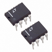
LT1001CN8 Linear Technology, LT1001CN8 Datasheet - Page 2

LT1001CN8
Manufacturer Part Number
LT1001CN8
Description
IC PRECISION OP-AMP SINGLE 8-DIP
Manufacturer
Linear Technology
Datasheet
1.LT1001CN8.pdf
(16 pages)
Specifications of LT1001CN8
Amplifier Type
General Purpose
Number Of Circuits
1
Slew Rate
0.25 V/µs
Gain Bandwidth Product
800kHz
Current - Input Bias
700pA
Voltage - Input Offset
18µV
Voltage - Supply, Single/dual (±)
±3 V ~ 18 V
Operating Temperature
0°C ~ 125°C
Mounting Type
Through Hole
Package / Case
8-DIP (0.300", 7.62mm)
Lead Free Status / RoHS Status
Contains lead / RoHS non-compliant
Current - Supply
-
Output Type
-
Current - Output / Channel
-
-3db Bandwidth
-
Available stocks
Company
Part Number
Manufacturer
Quantity
Price
Company:
Part Number:
LT1001CN8
Manufacturer:
LT
Quantity:
5 700
Part Number:
LT1001CN8
Manufacturer:
LINEAR/凌特
Quantity:
20 000
Company:
Part Number:
LT1001CN8#PBF
Manufacturer:
LT
Quantity:
706
Part Number:
LT1001CN8#PBF
Manufacturer:
LINEAR/凌特
Quantity:
20 000
Company:
Part Number:
LT1001CN8/NA
Manufacturer:
LT
Quantity:
1 400
Company:
Part Number:
LT1001CN8/NA
Manufacturer:
CSI
Quantity:
1 400
ABSOLUTE
PACKAGE/ORDER
LT1001
(Note 1)
Supply Voltage ...................................................... 22V
Differential Input Voltage ...................................... 30V
Input Voltage ........................................................ 22V
Output Short Circuit Duration ......................... Indefinite
Consult LTC Marketing for parts specified with wider operating temperature ranges.
ELECTRICAL CHARACTERISTICS
SYMBOL PARAMETER
V
I
I
e
e
A
CMRR
PSRR
R
2
temperature range, otherwise specifications are at T
OS
b
n
n
OS
VOL
in
Time
V
T
JMAX
OS
OFFSET ADJUST
= 150 C,
–IN
Input Offset Voltage
Long Term Input Offset Voltage
Stability
Input Offset Current
Input Bias Current
Input Noise Voltage
Input Noise Voltage Density
Large Signal Voltage Gain
Common Mode Rejection Ratio
Power Supply Rejection Ratio
Input Resistance Differential Mode
H PACKAGE METAL CAN
+IN
2
1
3
JA
Consider the N8 and S8 Packages for Alternate Source
V– (CASE)
TOP VIEW
= 150 C/W,
–
+
8
4
OBSOLETE PACKAGE
W
MAXIMUM
7
5
NC
6
jc
V+
= 45 C/W
OUT
W W
INFORMATION
U
RATINGS
PART NUMBER
LT1001AMH/883
LT1001MH
LT1001ACH
LT1001CH
CONDITIONS
Note 2
Notes 3 and 4
0.1Hz to 10Hz (Note 3)
f
f
R
R
V
V
O
O
L
L
CM
S
= 10Hz (Note 6)
= 1000Hz (Note 3)
= 3V to 18V
ORDER
W
= 13V
2k , V
1k V
U
LT1001AM/883
LT1001AC
A
O
O
= 25 C. V
= 10V
= 12V
The
U
S
denotes the specifications which apply over the full operating
= 15V, unless otherwise noted
Operating Temperature Range
Lead Temperature (Soldering, 10 sec.)................. 300 C
8 PIN PLASTIC DIP
V
TRIM
LT1001AM/LT1001M (OBSOLETE) .. – 55 C to 150 C
LT1001AC/LT1001C .............................. 0 C to 125 C
Storage: All Devices.......................... – 65 C to 150 C
OS
–IN
+IN
N8 PACKAGE
V–
T
T
T
JMAX
JMAX
JMAX
1
2
3
4
= 150 C,
= 150 C,
8 PIN HERMETIC DIP
= 150 C,
MIN
450
300
114
110
30
LT1001AM/883
J8 PACKAGE
TOP VIEW
+
–
Consider the N8 and S8 Packages for Alternate Source
LT1001AC
10.3
JA
JA
JA
TYP
800
500
126
123
100
10
0.2
0.3
0.5
0.3
9.6
7
OBSOLETE PACKAGE
= 130 C/W (N)
= 150 C/W (S)
= 100 C/W (J)
8 PIN PLASTIC SO
S8 PACKAGE
8
7
6
5
18.0
11.0
MAX
15
25
1.0
2.0
2.0
0.6
V
TRIM
V+
OUT
NC
OS
MIN
400
250
110
106
15
LT1001M/LT1001C
S8 PART MARKING
LT1001AMJ8/883
LT1001MJ8
LT1001ACJ8
LT1001CJ8
PART NUMBER
PART NUMBER
LT1001ACN8
LT1001CN8
LT1001CS8
10.5
TYP
800
500
126
123
18
80
0.3
0.4
0.7
0.3
9.8
ORDER
ORDER
1001
18.0
11.0
MAX
60
1.5
3.8
4.0
0.6
V/month
nV Hz
nV Hz
UNITS
V/mV
V/mV
1001fb
V
M
nA
nA
p-p
dB
dB
V


