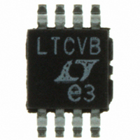
LTC6102HVCMS8#PBF Linear Technology, LTC6102HVCMS8#PBF Datasheet - Page 13

LTC6102HVCMS8#PBF
Manufacturer Part Number
LTC6102HVCMS8#PBF
Description
IC AMP CURRENT SENSE 8-MSOP
Manufacturer
Linear Technology
Datasheet
1.LTC6102CDDPBF.pdf
(26 pages)
Specifications of LTC6102HVCMS8#PBF
Amplifier Type
Current Sense
Number Of Circuits
1
Gain Bandwidth Product
200kHz
Current - Input Bias
60pA
Voltage - Input Offset
3µV
Current - Supply
420µA
Current - Output / Channel
1mA
Voltage - Supply, Single/dual (±)
5 V ~ 100 V
Operating Temperature
0°C ~ 70°C
Mounting Type
Surface Mount
Package / Case
8-MSOP, Micro8™, 8-uMAX, 8-uSOP,
Lead Free Status / RoHS Status
Lead free / RoHS Compliant
Output Type
-
-3db Bandwidth
-
Slew Rate
-
Available stocks
Company
Part Number
Manufacturer
Quantity
Price
APPLICATIONS INFORMATION
a signifi cant load on the power supply and create thermal
design headaches. In addition, heating in the sense resistor
can reduce its accuracy and reliability.
In contrast, the large dynamic range of the LTC6102 allows
the use of a much smaller sense resistor. The LTC6102
allows the minimum sense voltage to be reduced to less
than 10μV. The peak sense voltage would then be 10mV,
dissipating only 1W at 100A in a 100μΩ sense resistor!
With a specialized sense resistor, the same system would
allow peak currents of more than 1000A without exceeding
the input range of the LTC6102 or damaging the shunt.
Sense Resistor Connection
Kelvin connection of +IN and –INS to the sense resistor
should be used in all but the lowest power applications.
Solder connections and PC board interconnections that
carry high current can cause signifi cant error in measure-
ment due to their relatively large resistances. One 10mm
× 10mm square trace of one-ounce copper is approxi-
mately 0.5mΩ. A 1mV error can be caused by as little
as 2A fl owing through this small interconnect. This will
cause a 1% error in a 100mV signal. A 10A load current
in the same interconnect will cause a 5% error for the
same 100mV signal. An additional error is caused by the
change in copper resistance over temperature, which is in
excess of 0.4%/°C. By isolating the sense traces from the
110
100
90
80
70
60
50
40
30
20
0.001
DYNAMIC RANGE RELATIVE
TO 10μV, MINIMUM V
R
100dB: MAX
V
SENSE
SENSE
Dynamic Range vs Maximum
Power Dissipation in R
MAXIMUM POWER DISSIPATION (W)
R
MAX I
MAX I
MAX I
SENSE
0.01
= 1mΩ
= 1V
R
SENSE
SENSE
SENSE
SENSE
= 1Ω
R
SENSE
0.1
= 100mΩ
= 1A
= 10A
= 100A
SENSE
= 100μΩ
1
R
R
SENSE
SENSE
40dB: MAX
V
SENSE
SENSE
= 10μΩ
10
= 10mΩ
= 1mV
6102 AI01
100
Selection of External Input Resistor, R
The external input resistor, R
tance of the current sense circuit, I
example, if R
1mA for V
R
while limiting the output current. At low supply voltage,
I
high-current paths, this error can be reduced by orders of
magnitude. A sense resistor with integrated Kelvin sense
terminals will give the best results. Figure 2 illustrates the
recommended method. Note that the LTC6102 has a Kelvin
input structure such that current fl ows into –INF . The –INS
and –INF pins should be tied as close as possible to R
This reduces the parasitic series resistance so that R
may be as low as 1Ω, allowing high gain settings to be
used with very little gain error.
OUT
IN
should be chosen to provide the required resolution
may be as much as 1mA. By setting R
Figure 2. Kelvin Input Connection Preserves Accuracy
with Large Load Current and Large Output Current
R
SENSE
OUTPUT
LOAD
SENSE
LTC6102-1/LTC6102HV
V
+
R
IN
OUT
R
R
IN
IN
= 100, then I
V
= 100mV.
–
+
–
+IN
V
V
–
+
*VISHAY VCS1625 SERIES
WITH 4 PAD KELVIN CONNECTION
LTC6102
R
IN
TIE AS CLOSE TO R
+
–
LTC6102
IN
R
OUT
SENSE
, controls the transconduc-
–
= V
*
OUT
IN
R
SENSE
AS POSSIBLE
IN
V
–INS
V
OUT
LOAD
–INF
V
–
+
REG
C
+
= V
LTC6102
IN
REG
/100 or I
SENSE
R
OUT
6102 F02
IN
V
such that
OUT
/R
0.1μF
13
IN
OUT
. For
6102fd
IN
IN
=
.


