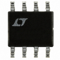
LT1208CS8#PBF Linear Technology, LT1208CS8#PBF Datasheet - Page 8

LT1208CS8#PBF
Manufacturer Part Number
LT1208CS8#PBF
Description
IC OP-AMP HI-SPEED DUAL 8SOIC
Manufacturer
Linear Technology
Datasheet
1.LT1208CS8PBF.pdf
(12 pages)
Specifications of LT1208CS8#PBF
Amplifier Type
General Purpose
Number Of Circuits
2
Slew Rate
400 V/µs
Gain Bandwidth Product
45MHz
Current - Input Bias
4µA
Voltage - Input Offset
1000µV
Current - Supply
7mA
Current - Output / Channel
40mA
Voltage - Supply, Single/dual (±)
5 V ~ 30 V, ±2.5 V ~ 15 V
Operating Temperature
0°C ~ 70°C
Mounting Type
Surface Mount
Package / Case
8-SOIC (3.9mm Width)
Lead Free Status / RoHS Status
Lead free / RoHS Compliant
Output Type
-
-3db Bandwidth
-
Available stocks
Company
Part Number
Manufacturer
Quantity
Price
LT1208/LT1209
A
8
Low Voltage Operation
The LT1208/LT1209 are functional at room temperature
with only 3V of total supply voltage. Under this condition,
however, the undistorted output swing is only 0.8V
more realistic condition is operation at 2.5V supplies (or
5V and ground). Under these conditions, at room tem-
perature, the typical input common-mode range is 1.9V to
–1.3V (for a V
wave can be faithfully reproduced. With 5V total supply
voltage the gain-bandwidth is reduced to 26MHz and the
slew rate is reduced to 135V/ s.
PPLICATI
A
A
V
V
= 1
= –1
Large-Signal Transient Response
Large-Signal Transient Response
OS
O
change of 1mV), and a 5MHz, 2V
U
S
I FOR ATIO
U
W
1208/09 AI04
1208/09 AI06
U
P-P
P-P
sine
. A
Power Dissipation
The LT1208/LT1209 combine high speed and large output
current drive in small packages. Because of the wide
supply voltage range, it is possible to exceed the maxi-
mum junction temperature under certain conditions.
Maximum junction temperature (T
ambient temperature (T
follows:
Maximum power dissipation occurs at the maximum
supply current and when the output voltage is at 1/2 of
either supply voltage (or the maximum swing if less than
1/2 supply voltage).
For each amplifier P
Example: LT1208 in S8 at 70 C, V
DAC Current-to-Voltage Converter
The wide bandwidth, high slew rate and fast settling time
of the LT1208/LT1209 make them well-suited for current-
to-voltage conversion after current output D/A converters.
A typical application with a DAC-08 type converter (full-
scale output of 2mA) uses a 5k feedback resistor. A 7pF
compensation capacitor across the feedback resistor is
used to null the pole at the inverting input caused by the
DAC output capacitance. The combination of the LT1208/
LT1209 and DAC settles to less than 40mV (1LSB) in
140ns for a 10V step.
P
LT1208CN8: T
LT1208CS8: T
LT1209CN:
LT1209CS:
P
T
DMAX
J
DMAX
= 70°C + (2
= (V
= (20V)(10.5mA) +
+
– V
T
T
J
J
J
J
DMAX
= T
= T
= T
= T
–
260mW)(150°C/W) = 148°C
)(I
A
A
A
A
A
SMAX
) and power dissipation (P
+ (P
+ (P
+ (P
+ (P
is as follows:
) +
D
D
D
D
500
(5V)
(0.5V
100 C/W)
150 C/W)
70 C/W)
100 C/W)
J
S
) is calculated from the
= 10V, R
R
2
L
+
= 260mW
)
2
L
= 500
D
) as


