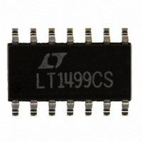
LT1499CS#PBF Linear Technology, LT1499CS#PBF Datasheet - Page 12

LT1499CS#PBF
Manufacturer Part Number
LT1499CS#PBF
Description
IC OP-AMP R-R IN/OUT QUAD 14SOIC
Manufacturer
Linear Technology
Series
C-Load™r
Datasheet
1.LT1498CN8PBF.pdf
(24 pages)
Specifications of LT1499CS#PBF
Amplifier Type
General Purpose
Number Of Circuits
4
Output Type
Rail-to-Rail
Slew Rate
6 V/µs
Gain Bandwidth Product
10.5MHz
Current - Input Bias
250nA
Voltage - Input Offset
200µV
Current - Supply
1.8mA
Current - Output / Channel
30mA
Voltage - Supply, Single/dual (±)
2.2 V ~ 36 V, ±1.1 V ~ 18 V
Operating Temperature
0°C ~ 70°C
Mounting Type
Surface Mount
Package / Case
14-SOIC (3.9mm Width), 14-SOL
Number Of Elements
4
Unity Gain Bandwidth Product
10.5MHz
Common Mode Rejection Ratio
81dB
Input Offset Voltage
0.475@5VmV
Input Bias Current
650nA
Single Supply Voltage (typ)
3/5/9/12/15/18/24/28V
Dual Supply Voltage (typ)
±3/±5/±9/±12V
Voltage Gain In Db
131.6dB
Power Supply Rejection Ratio
88dB
Power Supply Requirement
Single/Dual
Shut Down Feature
No
Single Supply Voltage (min)
2.2V
Single Supply Voltage (max)
30V
Dual Supply Voltage (min)
±1.1V
Dual Supply Voltage (max)
±15V
Technology
BiCOM
Operating Temp Range
0C to 70C
Operating Temperature Classification
Commercial
Mounting
Surface Mount
Pin Count
14
Package Type
SOIC N
Lead Free Status / RoHS Status
Lead free / RoHS Compliant
-3db Bandwidth
-
Lead Free Status / Rohs Status
Compliant
Available stocks
Company
Part Number
Manufacturer
Quantity
Price
ELECTRICAL CHARACTERISTICS
LT1498/LT1499
–55°C < T
SYMBOL
V
V
ΔV
I
ΔI
I
ΔI
A
CMRR
PSRR
V
V
I
I
GBW
SR
Note 1: Stresses beyond those listed under Absolute Maximum Ratings
may cause permanent damage to the device. Exposure to any Absolute
Maximum Rating condition for extended periods may affect device
reliability and lifetime.
Note 2: A heat sink may be required to keep the junction temperature
below the absolute maximum rating when the output is shorted
indefi nitely.
Note 3: This parameter is not 100% tested.
Note 4: The LT1498C/LT1499C are guaranteed to meet specifi ed
performance from 0°C to 70°C. The LT1498C/LT1499C are designed,
characterized and expected to meet specifi ed performance from –40°C
to 85°C but are not tested or QA sampled at these temperatures. The
LT1498I/LT1499I are guaranteed to meet specifi ed performance from
–40°C to 85°C. The LT1498H/LT1499H are guaranteed to meet specifi ed
performance from –40°C to 125°C. The LT1498MP is guaranteed to meet
specifi ed performance from –55°C to 125°C.
12
B
OS
SC
S
VOL
OS
OS
OL
OH
B
OS
OS
TC
A
PARAMETER
Input Offset Voltage
Input Offset Voltage Drift (Note 3)
Input Offset Voltage Shift
Input Offset Voltage Match (Channel-to-Channel) V
Input Bias Current
Input Bias Current Shift
Input Bias Current Match (Channel-to-Channel)
Input Offset Current
Input Offset Current Shift
Large-Signal Voltage Gain
Channel Separation
Common Mode Rejection Ratio
CMRR Match (Channel-to-Channel) (Note 5)
Power Supply Rejection Ratio
PSRR Match (Channel-to-Channel) (Note 5)
Output Voltage Swing (Low) (Note 6)
Output Voltage Swing (High) (Note 6)
Short-Circuit Current
Supply Current per Amplifi er
Gain-Bandwidth Product (Note 7)
Slew Rate
< 125°C. V
S
= ±15V, V
CM
= 0V, V
OUT
= 0V, unless otherwise noted. (Note 4)
CONDITIONS
V
V
V
V
V
V
V
V
V
V
V
V
V
V
V
V
V
V
No Load
I
I
No Load
I
I
A
Measure at V
SINK
SINK
SOURCE
SOURCE
CM
CM
CM
CM
CM
CM
CM
CM
CM
CM
CM
CM
CM
O
O
CM
CM
S
S
V
= –1, R
= –14.5V to 14.5V, R
= –10V to 10V, R
= ±5V to ±15V
= ±5V to ±15V
The
= V
= V
= V
= V
= V
= V
= V
= V
= V
= V
= V
= V
= V
= V
= V
= 0.5mA
= 10mA
+
–
+
–
–
+
–
–
+
–
+
–
–
–
–
= 0.5mA
= 10mA
l
– 0.5V
+ 0.5V
– 0.5V
+ 0.5V to V
+ 0.5V, V
– 0.5V
+ 0.5V
+ 0.5V to V
– 0.5V (Note 5)
+ 0.5V (Note 5)
– 0.5V
+ 0.5V
+ 0.5V to V
+ 0.5V to V
+ 0.5V to V
L
denotes the specifi cations which apply over the temperature range
= Open, V
O
= ±5V
Note 5: Matching parameters are the difference between amplifi ers A and
D and between B and C on the LT1499; between the two amplifi ers on the
LT1498.
Note 6: Output voltage swings are measured between the output and
power supply rails.
Note 7: V
5V tests.
Note 8: V
±15V tests.
+
L
– 0.5V (Note 5)
+
+
+
+
+
= 2k
O
– 0.5V
– 0.5V
– 0.5V
– 0.5V
– 0.5V
= ±10V
L
= 10k
S
S
= 3V, V
= 3V, V
S
S
= ±15V GBW limit guaranteed by correlation to
= 5V slew rate limit guaranteed by correlation to
l
l
l
l
l
l
l
l
l
l
l
l
l
l
l
l
l
l
l
l
l
l
l
l
l
l
l
l
l
l
–1200
–400
±7.5
MIN
110
5.8
2.2
40
86
80
88
80
0
0
–500
1000
4.75
TYP
350
350
250
400
500
–40
400
120
100
100
100
100
275
500
±12
1.0
2.0
3.5
2.5
8.5
40
40
40
80
25
50
65
1300
1300
1500
2200
1200
2400
1400
MAX
400
300
300
600
100
520
120
3.2
75
20
0
0
UNITS
14989fg
μV/°C
μV/°C
V/mV
MHz
V/μs
mV
mV
mV
mV
mV
mV
mA
mA
μV
μV
μV
μV
nA
nA
nA
nA
nA
nA
nA
nA
dB
dB
dB
dB
dB


