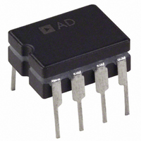
OP77EZ Analog Devices Inc, OP77EZ Datasheet

OP77EZ
Specifications of OP77EZ
Available stocks
Related parts for OP77EZ
OP77EZ Summary of contents
Page 1
FEATURES Outstanding gain linearity Ultrahigh gain, 5000 V/mV min Low V over temperature, 55 μV max OS Excellent TCV , 0.3 μV/°C max OS High PSRR, 3 μV/V max Low power consumption max Fits OP07, 725,108A/308A, 741 sockets ...
Page 2
OP77 TABLE OF CONTENTS Features .............................................................................................. 1 Pin Connections ............................................................................... 1 General Description ......................................................................... 1 Revision History ............................................................................... 2 Electrical Specifications ............................................................... 3 Wafer Test Limits .......................................................................... 4 Typical Electrical Characteristics ............................................... 5 Absolute Maximum Ratings ............................................................ 6 REVISION HISTORY ...
Page 3
ELECTRICAL SPECIFICATIONS @ V = ± 25°C, unless otherwise noted Table 1. Parameter INPUT OFFSET VOLTAGE 1 LONG-TERM STABILITY INPUT OFFSET CURRENT INPUT BIAS CURRENT 2 INPUT NOISE VOLTAGE INPUT NOISE VOLTAGE DENSITY 2 INPUT ...
Page 4
OP77 @ V = ±15 V, −25°C ≤ T ≤ +85°C for OP77FJ and OP77E/OP77F, unless otherwise noted Table 2. Parameter INPUT OFFSET VOLTAGE AVERAGE INPUT OFFSET VOLTAGE DRIFT INPUT OFFSET CURRENT AVERAGE INPUT OFFSET CURRENT DRIFT INPUT ...
Page 5
TYPICAL ELECTRICAL CHARACTERISTICS @ V = ± 25°C, unless otherwise noted Table 4. Parameter AVERAGE INPUT OFFSET VOLTAGE DRIFT NULLED INPUT OFFSET VOLTAGE DRIFT AVERAGE INPUT OFFSET CURRENT DRIFT SLEW RATE BANDWIDTH Symbol Conditions TCV ...
Page 6
OP77 ABSOLUTE MAXIMUM RATINGS Table 5. 1 Parameter Supply Voltage Differential Input Voltage 2 Input Voltage Output Short-Circuit Duration Storage Temperature Range Operating Temperature Range Junction Temperature ( Lead Temperature (Soldering, 60 sec) 1 Absolute Maximum Ratings apply ...
Page 7
TYPICAL PERFORMANCE CHARACTERISTICS ±15V 25° 10kΩ –1 –2 –10 –5 0 OUTPUT VOLTAGE (V) Figure 3. Gain Linearity (Input Voltage vs. Output Voltage ±15V S ...
Page 8
OP77 100 –20 10 100 1k 10k FREQUENCY (Hz) Figure 9. Closed-Loop Response for Various Gain Configurations 160 140 120 100 0.01 0 100 1k FREQUENCY (Hz) Figure ...
Page 9
V = ±15V 25° 0.1 100 1k 10k FREQUENCY (Hz) Figure 15. Input Wideband Noise vs. Bandwidth (0 Frequency Indicated) 1k RS1 = RS2 = 200kΩ THERMAL NOISE OF SOURCE EXCLUDED 100 ...
Page 10
OP77 TEST CIRCUITS 200kΩ 50Ω OP77 V OS Figure 21. Typical Offset Voltage Test Circuit 2.5MΩ V+ 100Ω 3.3kΩ 6 OP77 100Ω 3 4.7µF 4 (≈10Hz FILTER) V– V INPUT REFERRED NOISE = 25,000 Figure 22. Typical Low-Frequency ...
Page 11
APPLICATIONS R2 1MΩ +15V 0.1µF R1 1kΩ OP77E 0.1µF 1kΩ R4 1MΩ –15V Figure 27. Precision High-Gain Differential Amplifier The high gain, gain linearity, CMRR, and low TCV OP77 make it possible to obtain ...
Page 12
... In these circuits, the high gain, high CMRR, and low TCV the OP77 ensure high accuracy. The high gain and low TCV inputs from microvolts to volts. In Figure 33, the signal always appears as a common-mode signal to the op amps. The OP77EZ CMRR of 1 μV/V ensures errors of less than 2 ppm. 1kΩ +15V +15V C1 D1 0.1µ ...
Page 13
Figure 34 relies upon low TCV of the OP77 and noise OS combined with very high CMRR to provide precision buffering of the averaged REF-01 voltage outputs. 1kΩ Figure 35, C polyethylene to minimize dielectric absorption and ...
Page 14
OP77 C C +15V R 100kΩ 0.1µ 1kΩ 1N4148 OP77 2kΩ 0.1µF –15V Figure 36. Precision Threshold Detector/Amplifier When V < amplifier output swings negative, ...
Page 15
OUTLINE DIMENSIONS 0.1850 (4.70) 0.1650 (4.19) 0.0400 (1.02) MAX 0.0400 (1.02) 0.0100 (0.25) CONTROLLING DIMENSIONS ARE IN INCHES; MILLIMETER DIMENSIONS (IN PARENTHESES) ARE ROUNDED-OFF INCH EQUIVALENTS FOR REFERENCE ONLY AND ARE NOT APPROPRIATE FOR USE IN DESIGN. 0.005 (0.13) 0.055 ...
Page 16
... ORDERING GUIDE 1 Model Temperature Range OP77FJ −25°C to +85°C OP77FJZ −25°C to +85°C OP77EZ −25°C to +85°C OP77FZ −25°C to +85°C OP77NBC RoHS Compliant Part. ©2002–2010 Analog Devices, Inc. All rights reserved. Trademarks and registered trademarks are the property of their respective owners. ...


