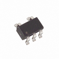
MAX4321EUK+T Maxim Integrated Products, MAX4321EUK+T Datasheet - Page 3

MAX4321EUK+T
Manufacturer Part Number
MAX4321EUK+T
Description
IC OP AMP R-R I/O LV SOT23-5
Manufacturer
Maxim Integrated Products
Datasheet
1.MAX4321EUKT.pdf
(12 pages)
Specifications of MAX4321EUK+T
Amplifier Type
General Purpose
Number Of Circuits
1
Output Type
Rail-to-Rail
Slew Rate
2 V/µs
Gain Bandwidth Product
5MHz
Current - Input Bias
50nA
Voltage - Input Offset
1200µV
Current - Supply
725µA
Current - Output / Channel
50mA
Voltage - Supply, Single/dual (±)
2.4 V ~ 6.5 V, ±1.2 V ~ 3.25 V
Operating Temperature
-40°C ~ 85°C
Mounting Type
Surface Mount
Package / Case
SOT-23-5, SC-74A, SOT-25
Number Of Channels
1
Voltage Gain Db
103 dB
Common Mode Rejection Ratio (min)
60 dB
Input Offset Voltage
3.5 mV
Operating Supply Voltage
3 V, 5 V
Supply Current
0.725 mA
Maximum Power Dissipation
571 mW
Maximum Operating Temperature
+ 85 C
Mounting Style
SMD/SMT
Maximum Dual Supply Voltage
+/- 3.25 V
Minimum Operating Temperature
- 40 C
Lead Free Status / RoHS Status
Lead free / RoHS Compliant
-3db Bandwidth
-
Lead Free Status / Rohs Status
Details
Other names
MAX4321EUK+T
MAX4321EUK+TTR
MAX4321EUK+TTR
DC ELECTRICAL CHARACTERISTICS
(V
AC ELECTRICAL CHARACTERISTICS
(V
Note 1: All devices are 100% production tested at T
Supply Voltage Range
Supply Current
Input Offset Voltage
Input Offset Voltage
Temperature Coefficient
Input Bias Current
Input Offset Current
Common-Mode Input Voltage
Range
Common-Mode Rejection Ratio
Power-Supply Rejection Ratio
Large-Signal Voltage Gain
Output Voltage Swing
Gain-Bandwidth Product
Phase Margin
Gain Margin
Total Harmonic Distortion
and Noise
Slew Rate
Settling Time to 0.01%
Turn-On Time
Input Capacitance
Input Noise Voltage Density
Input Noise Current Density
CC
CC
= +5.0V, V
= +5.0V, V
PARAMETER
PARAMETER
EE
EE
= 0, V
= 0, V
_______________________________________________________________________________________
CM
CM
= 0, V
= 0, V
Low-Cost, Low-Voltage, Rail-to-Rail,
OUT
OUT
SYMBOL
SYMBOL
Input/Output, SOT23 5MHz Op Amp
V
I
THD+N
t
CC
OFFSET
CMRR
SETTLE
PSRR
V
I
GBP
V
= V
V
= V
BIAS
I
t
C
A
SR
OUT
CC
ON
CM
OS
- V
IN
V
CC
CC
EE
/2, R
/2, R
V
V
V
V
Inferred from CMRR test
V
2.4V < V
V
R = 250Ω
10kHz tone, V
A
V
V
V
f = 1kHz
f = 1kHz
L
CM
CM
CM
CM
EE
OUT
L
OUT
OUT
CC
V
A
= ∞ connected to V
= 250Ω connected to V
= +1V/V
= +25°C. All temperature limits are guaranteed by design and characterization.
≤ V
= 0 to 3V step
= V
= V
= V
= V
= 0.40V to 4.60V, R
= 1V step
= 2V step, A
CM
OUT
EE
EE
EE
CC
≤ V
or V
or V
or V
< 6.5V
= V
OUT
CC
CC
CC
CC
CONDITIONS
CONDITIONS
CC
V
= 2Vpp,
/2
= +1V/V
CC
V
V
/2, T
L
CC
OL
CC
= 250Ω
- V
- V
/2, T A = +25°C, unless otherwise noted.)
A
EE
= -40°C to +85°C, unless otherwise noted.) (Note 1)
OH
MIN
MIN
V
2.4
54
62
66
EE
0.003
TYP
TYP
0.4
±2
64
12
22
5
2
2
1
3
±180
MAX
MAX
1200
V
±50
350
250
6.5
±6
CC
degrees
nV/√ Hz
pA/√Hz
UNITS
UNITS
V/μs
μV/°C
MHz
dB
μs
μs
pF
%
mV
mV
dB
dB
dB
μA
nA
nA
V
V
3


