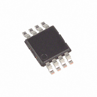
MAX4216EUA+ Maxim Integrated Products, MAX4216EUA+ Datasheet - Page 10

MAX4216EUA+
Manufacturer Part Number
MAX4216EUA+
Description
IC OP AMP R-R W/ENABLE 8-UMAX
Manufacturer
Maxim Integrated Products
Datasheet
1.MAX4213ESA.pdf
(16 pages)
Specifications of MAX4216EUA+
Amplifier Type
Voltage Feedback
Number Of Circuits
2
Output Type
Rail-to-Rail
Slew Rate
600 V/µs
-3db Bandwidth
200MHz
Current - Input Bias
5.4µA
Voltage - Input Offset
4000µV
Current - Supply
5.5mA
Current - Output / Channel
120mA
Voltage - Supply, Single/dual (±)
3.15 V ~ 11 V, ±1.575 V ~ 5.5 V
Operating Temperature
-40°C ~ 85°C
Mounting Type
Surface Mount
Package / Case
8-MSOP, Micro8™, 8-uMAX, 8-uSOP,
Number Of Channels
2
Voltage Gain Db
61 dB
Common Mode Rejection Ratio (min)
70 dB
Input Offset Voltage
4 mV
Operating Supply Voltage
3.3 V, 5 V
Maximum Power Dissipation
221 mW
Maximum Operating Temperature
+ 85 C
Mounting Style
SMD/SMT
Maximum Dual Supply Voltage
+/- 5.5 V
Minimum Operating Temperature
- 40 C
Lead Free Status / RoHS Status
Lead free / RoHS Compliant
Gain Bandwidth Product
-
Lead Free Status / Rohs Status
Details
The MAX4212/MAX4213/MAX4216/MAX4218/MAX4220
are single-supply, rail-to-rail, voltage-feedback ampli-
fiers that employ current-feedback techniques to
achieve 600V/µs slew rates and 300MHz bandwidths.
Excellent harmonic distortion and differential gain/
phase performance make these amplifiers an ideal
choice for a wide variety of video and RF signal-
processing applications.
The output voltage swing comes to within 50mV of each
supply rail. Local feedback around the output stage
assures low open-loop output impedance to reduce
gain sensitivity to load variations. This feedback also
produces demand-driven current bias to the output
transistors for ±100mA drive capability, while constrain-
ing total supply current to less than 7mA. The input
stage permits common-mode voltages beyond the nega-
tive supply and to within 2.25V of the positive supply rail.
The MAX4212/MAX4213/MAX4216/MAX4218/MAX4220
are internally compensated for unity gain. When config-
ured for unity gain, the devices require a 24
(R
Miniature, 300MHz, Single-Supply,
Rail-to-Rail Op Amps with Enable
Figure 1a. Noninverting Gain Configuration
10
_______________Detailed Description
__________Applications Information
F
) in series with the feedback path. This resistor
______________________________________________________________________________________
R
G
IN
R
TIN
R
F
V
OUT
Choosing Resistor Values
= [1+ (R
F
Unity-Gain Configuration
/ R
R
TO
G
)] V
IN
resistor
V
OUT
R
O
improves AC response by reducing the Q of the parallel
LC circuit formed by the parasitic feedback capaci-
tance and inductance.
Select the gain-setting feedback (R
resistor values to fit your application. Large resistor val-
ues increase voltage noise and interact with the amplifi-
er’s input and PC board capacitance. This can
generate undesirable poles and zeros and decrease
bandwidth or cause oscillations. For example, a nonin-
verting gain-of-two configuration (R
resistors, combined with 1pF of amplifier input capaci-
tance and 1pF of PC board capacitance, causes a pole
at 159MHz. Since this pole is within the amplifier band-
width, it jeopardizes stability. Reducing the 1k
tors to 100
but could limit output swing by adding 200
with the amplifier’s load resistor. Table 1 shows sug-
gested feedback, gain resistors, and bandwidth for
several gain values in the configurations shown in
Figures 1a and 1b.
These amplifiers operate from a single 3.3V to 11V power
supply or from dual supplies to ±5.5V. For single-supply
operation, bypass V
as close to the pin as possible. If operating with dual sup-
plies, bypass each supply with a 0.1µF capacitor.
Figure 1b. Inverting Gain Configuration
R
IN
TIN
Layout and Power-Supply Bypassing
R
G
Inverting and Noninverting Configurations
R
S
extends the pole frequency to 1.59GHz,
CC
V
R
OUT
F
to ground with a 0.1µF capacitor
= -(R
F
/ R
G
) V
IN
R
TO
F
F
= R
) and input (R
G
) using 1k
in parallel
V
OUT
resis-
R
O
G
)


