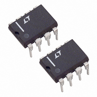
LT1672CN8 Linear Technology, LT1672CN8 Datasheet - Page 9

LT1672CN8
Manufacturer Part Number
LT1672CN8
Description
IC OPAMP R-R IN/OUT SNGL 8-DIP
Manufacturer
Linear Technology
Series
Over-The-Top®r
Datasheet
1.LT1673CS8PBF.pdf
(12 pages)
Specifications of LT1672CN8
Amplifier Type
General Purpose
Number Of Circuits
1
Output Type
Rail-to-Rail
Slew Rate
0.005 V/µs
Gain Bandwidth Product
12kHz
Current - Input Bias
25pA
Voltage - Input Offset
200µV
Current - Supply
1.9µA
Current - Output / Channel
1.5mA
Voltage - Supply, Single/dual (±)
2.2 V ~ 36 V, ±1.1 V ~ 18 V
Operating Temperature
0°C ~ 70°C
Mounting Type
Through Hole
Package / Case
8-DIP (0.300", 7.62mm)
Lead Free Status / RoHS Status
Contains lead / RoHS non-compliant
-3db Bandwidth
-
Available stocks
Company
Part Number
Manufacturer
Quantity
Price
Part Number:
LT1672CN8#PBF
Manufacturer:
LINEAR/凌特
Quantity:
20 000
APPLICATIO S I FOR ATIO
The device will not be damaged if the inputs are taken lower
than 300mV below the negative supply as long as the cur-
rent out of the pin is limited to less than 10mA. However,
the output phase is not guaranteed and the supply current
will increase.
Output
The graph, Capacitive Load Handling, shows amplifier sta-
bility with the output biased at half supply. If the output is
to be operated within about 100mV of the positive rail, the
allowable load capacitance is less. With this output volt-
age, the worst case occurs at A
the load capacitance should be less than 500pF with a 5V
supply and less than 100pF with a 30V supply.
Rail-to-Rail Operation
The simplified schematic, Figure 3, details the circuit
design approach of the LT1672/LT1673/LT1674. The
amplifier topology is a three-stage design consisting of a
rail-to-rail input stage, that continues to operate with the
inputs above the positive rail, a folded cascode second
stage that develops most of the voltage gain, and a rail-to-
rail common emitter stage that provides the current gain.
The input stage is formed by two diff amps Q1-Q2 and Q3-
Q6. For signals with a common mode voltage between V
IN
IN
+
–
Q1
Q10
Q2
U
U
Q5
Q3
D1
Q9
V
= 5 and light loads, where
Q4
W
Q6
D2
Q7
Q8
(V
Figure 3. Simplified Schematic
U
+
) – 0.8V
EE
Q16
D3
and (V
common mode exceeds (V
diverting the current from diff amp Q1-Q2 to current
mirror Q8-Q9. The current from Q8 biases on the other
diff amp consisting of PNP’s Q5-Q6 and NPN’s Q3-Q4.
Though Q5-Q6 are driven from the emitters rather than
the base, the basic diff amp action is the same. When the
common mode voltage is between (V
devices Q3 and Q4 act as followers, forming a buffer
between the amplifier inputs and the emitters of the Q5-
Q6. If the common mode voltage is taken above V
Schottky diodes D1 and D2 reverse bias and devices Q3
and Q4 then act as diodes. The diff amp formed by Q5-Q6
operates normally, however, the input bias current in-
creases to the emitter current of Q5-Q6, which is typically
180nA. The graph, Input Bias Current vs Common Mode
Voltage found in the Typical Performance Characteristics
section, shows these transitions at three temperatures.
The collector currents of the two-input pairs are combined
in the second stage consisting of Q11 to Q16, which
furnishes most of the voltage gain. Capacitor C1 sets the
amplifier bandwidth. The output stage is configured for
maximum swing by the use of common emitter output
devices Q21 and Q22. Diodes D4 to D6 and current source
Q15 set the output quiescent current.
Q11
Q13
R1
CC
Q12
Q14
R2
– 0.8V), Q1 and Q2 are active. When the input
Q17
I
2
C1
LT1672/LT1673/LT1674
Q15
D4
D5
D6
+
D7
I
1
CC
– 0.8V), Q7 turns on,
Q19
Q20
Q18
CC
– 0.8V) and V
Q21
Q22
1672/3/4 F03
OUT
9
CC
CC
,
,


