AD8515ARTZ-R2 Analog Devices Inc, AD8515ARTZ-R2 Datasheet - Page 2
AD8515ARTZ-R2
Manufacturer Part Number
AD8515ARTZ-R2
Description
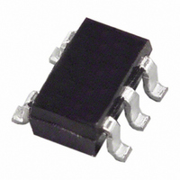
IC AMP GP R-R CMOS 5MHZ SOT23-5
Manufacturer
Analog Devices Inc
Datasheet
1.AD8515ARTZ-REEL7.pdf
(16 pages)
Specifications of AD8515ARTZ-R2
Slew Rate
2.7 V/µs
Design Resources
Extending the Capacitive Input Range of AD7745/AD7746 (CN0129)
Amplifier Type
General Purpose
Number Of Circuits
1
Output Type
Rail-to-Rail
Gain Bandwidth Product
5MHz
Current - Input Bias
5pA
Voltage - Input Offset
1000µV
Current - Supply
410µA
Current - Output / Channel
20mA
Voltage - Supply, Single/dual (±)
1.8 V ~ 5 V
Operating Temperature
-40°C ~ 125°C
Mounting Type
Surface Mount
Package / Case
SOT-23-5, SC-74A, SOT-25
Op Amp Type
Low Power
No. Of Amplifiers
1
Bandwidth
5MHz
Supply Voltage Range
1.8V To 5V
Amplifier Case Style
SOT-23
No. Of Pins
5
Lead Free Status / RoHS Status
Lead free / RoHS Compliant
-3db Bandwidth
-
Lead Free Status / RoHS Status
Lead free / RoHS Compliant, Lead free / RoHS Compliant
Other names
AD8515ARTZ-R2TR
Available stocks
Company
Part Number
Manufacturer
Quantity
Price

Part Number:
AD8515ARTZ-R2
Manufacturer:
ADI/亚德诺
Quantity:
20 000


AD8515
TABLE OF CONTENTS
Features .............................................................................................. 1
Applications....................................................................................... 1
Pin Configuration............................................................................. 1
General Description ......................................................................... 1
Revision History ............................................................................... 2
Specifications..................................................................................... 3
Absolute Maximum Ratings............................................................ 6
REVISION HISTORY
7/07—Rev. C to Rev. D
Updated Format..................................................................Universal
Updated Package Designator Throughout.................................... 1
Changes to Table 1, Supply Current/Amplifier ............................ 3
Changes to Table 2, Supply Current/Amplifier ............................ 4
Changes to Table 3, Large Signal Voltage Gain, Power Supply
Rejection Ratio, and Supply Current/Amplifier........................... 5
Changes to Figure 10........................................................................ 8
Changes to Figure 35...................................................................... 14
Updated Outline Dimensions ....................................................... 16
Changes to Ordering Guide .......................................................... 16
3/05—Rev. B to Rev. C
Changes to Specifications ................................................................ 2
Changes to Ordering Guide ............................................................ 5
4/03—Rev. A to Rev. B
Change to Figure 5 ......................................................................... 12
Electrical Characteristics............................................................. 3
Thermal Resistance ...................................................................... 6
ESD Caution.................................................................................. 6
Rev. D | Page 2 of 16
Typical Performance Characteristics ..............................................7
Theory of Operation ...................................................................... 12
Driving Capacitive Loads .............................................................. 13
A Micropower Reference Voltage Generator.............................. 14
Outline Dimensions ....................................................................... 16
2/03—Rev. 0 to Rev. A
Added new SC70 Package .................................................Universal
Changes to Features ..........................................................................1
Changes to General Description .....................................................1
Changes to Pin Configuration .........................................................1
Changes to Specifications.................................................................2
Changes to Absolute Maximum Ratings........................................5
Changes to Ordering Guide .............................................................5
Changes to TPC 3..............................................................................6
Changes to TPC 10............................................................................7
Changes to TPC 13............................................................................8
Changes to TPC 27......................................................................... 10
Changes to TPC 28......................................................................... 10
Added new TPC 29 ........................................................................ 10
Changes to Functional Description ............................................. 11
Updated to Outline Dimensions .................................................. 14
8/02—Revision. 0: Initial Version
Power Consumption vs. Bandwidth ........................................ 12
Full Power Bandwidth ............................................................... 13
A 100 kHz Single-Supply Second-Order Band-Pass Filter ... 14
Wien Bridge Oscillator .............................................................. 15
Ordering Guide .......................................................................... 16
Related parts for AD8515ARTZ-R2
Image
Part Number
Description
Manufacturer
Datasheet
Request
R

Part Number:
Description:
±1.7g Dual-Axis IMEMS Accelerometer Evaluation Board
Manufacturer:
Analog Devices Inc
Datasheet:

Part Number:
Description:
Inertial Sensor Evaluation System
Manufacturer:
Analog Devices Inc
Datasheet:
Part Number:
Description:
Manufacturer:
Analog Devices Inc
Datasheet:
Part Number:
Description:
Manufacturer:
Analog Devices Inc
Datasheet:
Part Number:
Description:
Manufacturer:
Analog Devices Inc
Datasheet:
Part Number:
Description:
Manufacturer:
Analog Devices Inc
Datasheet:
Part Number:
Description:
Manufacturer:
Analog Devices Inc
Datasheet:
Part Number:
Description:
Manufacturer:
Analog Devices Inc
Datasheet:
Part Number:
Description:
Manufacturer:
Analog Devices Inc
Datasheet:
Part Number:
Description:
Manufacturer:
Analog Devices Inc
Datasheet:
Part Number:
Description:
Manufacturer:
Analog Devices Inc
Datasheet:
Part Number:
Description:
Manufacturer:
Analog Devices Inc
Datasheet:
Part Number:
Description:
Manufacturer:
Analog Devices Inc
Datasheet: