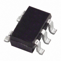
ADA4505-1ARJZ-R2 Analog Devices Inc, ADA4505-1ARJZ-R2 Datasheet - Page 15

ADA4505-1ARJZ-R2
Manufacturer Part Number
ADA4505-1ARJZ-R2
Description
IC OPAMP GP RRIO 50KHZ SOT23-5
Manufacturer
Analog Devices Inc
Datasheet
1.ADA4505-1ARJZ-R2.pdf
(24 pages)
Specifications of ADA4505-1ARJZ-R2
Slew Rate
0.006 V/µs
Amplifier Type
Voltage Feedback
Number Of Circuits
1
Output Type
Rail-to-Rail
Gain Bandwidth Product
50kHz
Current - Input Bias
0.5pA
Voltage - Input Offset
500µV
Current - Supply
9µA
Current - Output / Channel
40mA
Voltage - Supply, Single/dual (±)
1.8 V ~ 5 V, ±0.9 V ~ 2.5 V
Operating Temperature
-40°C ~ 125°C
Mounting Type
Surface Mount
Package / Case
SOT-23-5, SC-74A, SOT-25
Op Amp Type
Low Power
No. Of Amplifiers
1
Bandwidth
50kHz
Supply Voltage Range
± 0.9V To ± 2.5V
Amplifier Case Style
SOT-23
No. Of Pins
5
Lead Free Status / RoHS Status
Lead free / RoHS Compliant
-3db Bandwidth
-
Lead Free Status / RoHS Status
Lead free / RoHS Compliant, Lead free / RoHS Compliant
Other names
ADA4505-1ARJZ-R2TR
Available stocks
Company
Part Number
Manufacturer
Quantity
Price
Part Number:
ADA4505-1ARJZ-R2
Manufacturer:
ADI/亚德诺
Quantity:
20 000
Figure 55 displays a typical front-end section of an operational
amplifier with an on-chip charge pump.
Figure 56 shows the typical response of two devices from Figure 12,
which shows the input offset voltage vs. input common-mode
voltage for 10 devices. Figure 56 is expanded to make it easier to
compare with Figure 54, which shows the typical input offset
voltage vs. common-mode voltage response in a dual differential
pair input stage op amp.
V
BIAS
V
+IN
PP
Figure 55. Typical Front-End Section of an Op Amp
V
PP
Q1
= POSITIVE PUMPED VOLTAGE = V
with Embedded Charge Pump
Q2
–IN
V
V
DD
SS
RAIL-TO-RAIL
CASCODE
OUTPUT
STAGE
STAGE
AND
DD
+ 1.8V
OUT
Rev. D | Page 15 of 24
This solution improves the CMRR performance tremendously.
For example, if the input varies from rail to rail on a 2.5 V
supply rail, using a part with a CMRR of 70 dB minimum,
an input-referred error of 790 μV is introduced. Another part
with a CMRR of 52 dB minimum generates a 6.3 mV error.
The ADA4505-x family CMRR of 90 dB minimum causes only
a 79 μV error. As with the PSRR error, there are complex ways
to minimize this error, but the ADA4505-x family solves this
problem without incurring unnecessary circuitry complexity or
increased cost.
Figure 56. Input Offset Voltage vs. Input Common-Mode Voltage Response
–100
–150
–200
–250
–300
(Powered by a 5 V Supply; Results of Two Units Are Displayed)
300
250
200
150
100
–50
50
ADA4505-1/ADA4505-2/ADA4505-4
0
0
V
T
SY
A
0.5
= 25°C
= 5V
1.0
1.5
2.0
V
CM
2.5
(V)
3.0
3.5
4.0
4.5
5.0


