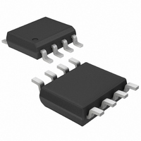
MAX4201ESA+ Maxim Integrated Products, MAX4201ESA+ Datasheet - Page 2

MAX4201ESA+
Manufacturer Part Number
MAX4201ESA+
Description
IC BUFFER OPEN LOOP 8-SOIC
Manufacturer
Maxim Integrated Products
Datasheet
1.MAX4200ESA.pdf
(14 pages)
Specifications of MAX4201ESA+
Amplifier Type
Buffer
Number Of Circuits
1
Slew Rate
4200 V/µs
-3db Bandwidth
780MHz
Current - Input Bias
800nA
Voltage - Input Offset
1000µV
Current - Supply
2.2mA
Current - Output / Channel
52mA
Voltage - Supply, Single/dual (±)
±4 V ~ 5.5 V
Operating Temperature
-40°C ~ 85°C
Mounting Type
Surface Mount
Package / Case
8-SOIC (3.9mm Width)
Number Of Channels
1
Input Offset Voltage
1 mV
Input Bias Current (max)
800 nA
Maximum Power Dissipation
471 mW
Maximum Operating Temperature
+ 85 C
Minimum Operating Temperature
- 40 C
Dual Supply Voltage
+/- 5 V
Maximum Dual Supply Voltage
+/- 5.5 V
Minimum Dual Supply Voltage
+/- 4 V
Mounting Style
SMD/SMT
Shutdown
No
Voltage Gain Db
6.02 dB
No. Of Amplifiers
1
Gain Bandwidth
780MHz
Supply Voltage Range
± 4V To ± 5.5V
Output Current
52mA
Amplifier Output
Single Ended
Rohs Compliant
Yes
Lead Free Status / RoHS Status
Lead free / RoHS Compliant
Output Type
-
Gain Bandwidth Product
-
Lead Free Status / Rohs Status
Lead free / RoHS Compliant
ABSOLUTE MAXIMUM RATINGS
Supply Voltage (V
Voltage on Any Pin to GND..............(V
Output Short-Circuit Duration to GND........................Continuous
Continuous Power Dissipation (T
Ultra-High-Speed, Low-Noise, Low-Power,
SOT23 Open-Loop Buffers
DC ELECTRICAL CHARACTERISTICS
(V
Stresses beyond those listed under “Absolute Maximum Ratings” may cause permanent damage to the device. These are stress ratings only, and functional
operation of the device at these or any other conditions beyond those indicated in the operational sections of the specifications is not implied. Exposure to
absolute maximum rating conditions for extended periods may affect device reliability.
2
Operating Supply Voltage
Quiescent Supply Current
Input Offset Voltage
Input Offset Voltage Drift
Input Offset Voltage
Matching
Input Bias Current
Input Resistance
Voltage Gain
Power-Supply Rejection
Output Resistance
Output Current
Short-Circuit Output
Current
Output-Voltage Swing
5-Pin SOT23 (derate 7.1mW/°C above +70°C).............571mW
8-Pin µMAX (derate 4.1mW/°C above +70°C) ..............330mW
8-Pin SO (derate 5.9mW/°C above +70°C)...................471mW
CC
_______________________________________________________________________________________
= +5V, V
PARAMETER
EE
= -5V, R
CC
to V
EE
L
= ∞, T
)................................................+12V
SYMBOL
A
TCV
A
R
V
I
= +70°C)
V
PSR
R
OUT
I
V
A
OUT
OUT
= T
I
I
SC
OS
S
B
IN
S
V
OS
EE
MIN
- 0.3V) to (V
to T
Guaranteed by PSR test
Per buffer, V
V
V
MAX4203/MAX4204/MAX4205
(Note 1)
-3.0V ≤
V
3.0V
V
f = DC
R
Sinking or sourcing
MAX4200/MAX4203
MAX4201/MAX4204
MAX4202/MAX4205
IN
IN
OUT
S
L
= ±4V to ±5.5V
MAX
= 30Ω
= 0V
= 0V
≤
, unless otherwise noted. Typical values are at T
CC
IN
+ 0.3V)
MAX4200/MAX4203, R
MAX4201/MAX4204, R
MAX4202/MAX4205, R
= 0V
CONDITIONS
Operating Temperature Range ...........................-40°C to +85°C
Storage Temperature Range .............................-65°C to +150°C
Lead Temperature (soldering, 10s) .................................+300°C
MAX4200/MAX4203
MAX4201/MAX4204
MAX4202/MAX4205
MAX4200/MAX4203
MAX4201/MAX4204
MAX4202/MAX4205
MAX4200/MAX4203
MAX4201/MAX4204
MAX4202/MAX4205
R
R
R
R
R
L
L
L
L
L
= 150Ω
= 100Ω
= 37.5Ω
= 50Ω
= 75Ω
EXT
EXT
EXT
= 150Ω
= 50Ω
= 75Ω
±3.3
±3.2
±1.9
±2.0
0.42
0.41
MIN
0.9
±4
A
55
= +25°C.)
±3.8
±3.7
±3.3
±2.1
±2.3
TYP
0.96
0.50
0.50
±90
±52
±44
500
150
2.2
0.4
0.8
20
72
50
75
90
75
1
8
MAX
±5.5
0.58
0.59
1.1
15
10
4
UNITS
µV/°C
mA
V/V
mA
mA
mV
mV
µA
kΩ
dB
Ω
V
V


