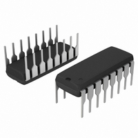
NE5517ANG ON Semiconductor, NE5517ANG Datasheet - Page 10

NE5517ANG
Manufacturer Part Number
NE5517ANG
Description
IC AMP XCONDUCTANCE DUAL 16-DIP
Manufacturer
ON Semiconductor
Datasheet
1.NE5517DG.pdf
(14 pages)
Specifications of NE5517ANG
Amplifier Type
Transconductance
Number Of Circuits
2
Output Type
Push-Pull
Slew Rate
50 V/µs
Gain Bandwidth Product
2MHz
Current - Input Bias
400nA
Voltage - Input Offset
400µV
Current - Supply
2.6mA
Current - Output / Channel
650µA
Voltage - Supply, Single/dual (±)
4 V ~ 44 V, ±2 V ~ 22 V
Operating Temperature
0°C ~ 70°C
Mounting Type
Through Hole
Package / Case
16-DIP (0.300", 7.62mm)
Number Of Channels
2
Input Offset Voltage
2 mV
Supply Voltage (max)
44 V
Supply Current
2.6 mA
Common Mode Rejection Ratio (min)
80 dB
Input Voltage Range (max)
Positive Rail - 3 V
Mounting Style
Through Hole
Maximum Operating Temperature
+ 70 C
Minimum Operating Temperature
0 C
Maximum Power Dissipation
1500 mW
Lead Free Status / RoHS Status
Lead free / RoHS Compliant
-3db Bandwidth
-
Lead Free Status / Rohs Status
Lead free / RoHS Compliant
Other names
NE5517ANG
NE5517ANGOS
NE5517ANGOS
Voltage-Controlled Resistor (VCR)
proportional to the input voltage, a voltage variable resistor
can be made. Figure 26 shows how this is done. A voltage
presented at the R
This voltage is multiplied by g
through the R
where g
temperature. Figure 27 shows a Voltage Controlled Resistor
using linearizing diodes. This improves the noise
performance of the resistor.
Voltage-Controlled Filters
The circuit is a unity gain buffer until X
R/R
octave with the −3 dB point being defined by the given
equations. Operating in the same manner, a Voltage
Controlled High-Pass Filter is shown in Figure 29. Higher
order filters can be made using additional amplifiers as
shown in Figures 30 and 31.
Because an OTA is capable of producing an output current
Figure 28 shows a Voltage Controlled Low-Pass Filter.
A
. Then, the frequency response rolls off at a 6dB per
M
is approximately 19.21 mMHOs at room
X
terminals:
X
terminals forces a voltage at the input.
R
x
+
200W
g
R ) R
M
M
) R
200W
and thereby forces a current
V
OS
I
A
D
A
2
3
4
R
1kW
P
C
+
−
NE5517/A
Figure 27. VCR with Linearizing Diodes
+V
/g
NE5517, NE5517A, AU5517
−V
CC
+V
M
2
CC
CC
11
3
4
is equal to
NE5517/A
−V
http://onsemi.com
+V
CC
CC
11
6
Figure 26. VCR
I
O
5
10
1
R
X
Voltage-Controlled Oscillators
wave generator. With the indicated values a range from
2.0 Hz to 200 kHz is possible by varying I
to 10 mA.
to be above 5.0 V.
sawtooth pulse generator, as shown in Figure 33.
APPLICATION HINTS
I
mirror ratio should be as accurate as possible over the entire
current range. A current mirror with only two transistors is
not recommended. A suitable current mirror can be built
with a PNP transistor array which causes excellent matching
and thermal coupling among the transistors. The output
current range of the DAC normally reaches from 0 to
−2.0 mA. In this application, however, the current range is
set through R
ABC
30kW
C
Figure 32 shows a voltage-controlled triangle-square
The output amplitude is determined by I
Please notice the differential input voltage is not allowed
With a slight modification of this circuit you can get the
To hold the transconductance g
5
7
100kW
should be chosen not greater than 1.0 mA. The current
R
X
R
8
C
I
30kW
DACMAX
7
100kW
REF
R
8
10kW
+ 2 @
(10 kW) to 0 to −1.0 mA.
V
V
−V
+V
INT
C
INT
OUT
10kW
CC
CC
R
V
REF
R
REF
X
−V
+V
INT
V
INT
+
+ 2 @ 5V
C
CC
CC
R ) R A
g M @ R A
M
10kW
within the linear range,
ABC
+ 1mA
OUT
from 1.0 mA
× R
OUT
.


