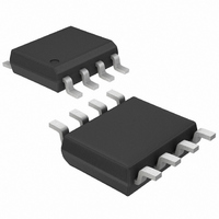
MAX4489ASA+ Maxim Integrated Products, MAX4489ASA+ Datasheet - Page 10

MAX4489ASA+
Manufacturer Part Number
MAX4489ASA+
Description
IC OP AMP R-R LN 42MHZ 8-SOIC
Manufacturer
Maxim Integrated Products
Datasheet
1.MAX4477AUA.pdf
(21 pages)
Specifications of MAX4489ASA+
Amplifier Type
General Purpose
Number Of Circuits
2
Output Type
Rail-to-Rail
Slew Rate
10 V/µs
Gain Bandwidth Product
42MHz
Current - Input Bias
1pA
Voltage - Input Offset
70µV
Current - Supply
2.5mA
Current - Output / Channel
48mA
Voltage - Supply, Single/dual (±)
2.7 V ~ 5.5 V, ±1.35 V ~ 2.75 V
Operating Temperature
-40°C ~ 125°C
Mounting Type
Surface Mount
Package / Case
8-SOIC (3.9mm Width)
Number Of Channels
2
Voltage Gain Db
120 dB
Common Mode Rejection Ratio (min)
90 dB
Input Offset Voltage
0.35 mV
Operating Supply Voltage
3 V, 5 V
Maximum Power Dissipation
471 mW
Maximum Operating Temperature
+ 125 C
Mounting Style
SMD/SMT
Minimum Operating Temperature
- 40 C
Lead Free Status / RoHS Status
Lead free / RoHS Compliant
-3db Bandwidth
-
Lead Free Status / Rohs Status
Details
SOT23, Low-Noise, Low-Distortion,
Wide-Band, Rail-to-Rail Op Amps
The amplifier’s input-referred noise-voltage density is
dominated by flicker noise at lower frequencies, and by
thermal noise at higher frequencies. Because the ther-
mal noise contribution is affected by the parallel combi-
nation of the feedback resistive network (R
Figure 1), these resistors should be reduced in cases
where the system bandwidth is large and thermal noise
is dominant. This noise contribution factor decreases,
however, with increasing gain settings.
For example, the input noise-voltage density of the cir-
cuit with R
e n = 14nV/√Hz, e n can be reduced to 6nV/√Hz by
choosing R
expense of greater current consumption and potentially
higher distortion. For a gain of 100V/V with R
R
The amplifier’s input capacitance is 10pF. If the resis-
tance seen by the inverting input is large (feedback
network), this can introduce a pole within the amplifier’s
bandwidth resulting in reduced phase margin.
Compensate the reduced phase margin by introducing
a feed-forward capacitor (C
input and the output (Figure 1). This effectively cancels
the pole from the inverting input of the amplifier.
Choose the value of C
In the unity-gain stable MAX4475–MAX4478, the use of
a proper C
A
MAX4489, C
Figures 2a and 2b show transient response both with
and without C
Using a slightly smaller C
mula above achieves a higher bandwidth at the
expense of reduced phase and gain margin. As a gen-
eral guideline, consider using C
R
greater than 5kΩ (MAX4488/MAX4489).
The MAX4475–MAX4478/MAX4488/MAX4489 combine
good driving capability with ground-sensing input and
rail-to-rail output operation. With their low distortion and
low noise, they are ideal for use in ADC buffers, med-
ical instrumentation systems and other noise-sensitive
applications.
10
G
F
V
= 1.1kΩ, the e n is still a low 6nV/√Hz.
is greater than 20kΩ (MAX4475–MAX4478) or
= -1V/V. In the decompensated MAX4488/
______________________________________________________________________________________
Using a Feed-Forward Compensation
F
F
Z
= 10kΩ, R
Z
= 100kΩ, R
Z
is most important for A
.
Applications Information
C
is most important for A
Z
= 10 x (R
Z
G
as follows:
= 1.1kΩ (A
Z
G
than suggested by the for-
F
= 11kΩ (A
Z
/ R
) between the inverting
Z
G
for cases where R
) [pF]
V
Capacitor, C
V
= +5V/V), at the
V
= +2V/V, and
Low Noise
V
= +5V/V) is
= +10V/V.
F
= 100kΩ,
F
|| R
G
G
Z
||
,
The common-mode input range of these devices
extends below ground, and offers excellent common-
mode rejection. These devices are guaranteed not to
undergo phase reversal when the input is overdriven
(Figure 3).
Figure 4 showcases the true rail-to-rail output operation
of the amplifier, configured with A
swings to within 8mV of the supplies with a 10kΩ load,
making the devices ideal in low-supply voltage applica-
tions.
The MAX4475–MAX4478/MAX4488/MAX4489 operate
from a single +2.7V to +5.5V power supply or from dual
supplies of ±1.35V to ±2.75V. For single-supply opera-
tion, bypass the power supply with a 0.1µF ceramic
Figure 3. Overdriven Input Showing No Phase Reversal
Figure 4. Rail-to-Rail Output Operation
Ground-Sensing and Rail-to-Rail Outputs
5V
0V
0V
A
V
R
V
DD
L
= 10kΩ
= +1
= +5V
Power Supplies and Layout
20µs/div
40µs/div
V
= 5V/V. The output
V
1V/div
V
2V/div
V
2V/div
OUT
IN
OUT


