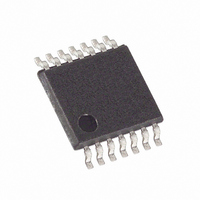
MAX4454EUD+ Maxim Integrated Products, MAX4454EUD+ Datasheet - Page 12

MAX4454EUD+
Manufacturer Part Number
MAX4454EUD+
Description
IC OP AMP R-R SS 14-TSSOP
Manufacturer
Maxim Integrated Products
Datasheet
1.MAX4352EXKT.pdf
(19 pages)
Specifications of MAX4454EUD+
Amplifier Type
Voltage Feedback
Number Of Circuits
4
Output Type
Rail-to-Rail
Slew Rate
95 V/µs
-3db Bandwidth
200MHz
Current - Input Bias
800nA
Voltage - Input Offset
400µV
Current - Supply
620µA
Current - Output / Channel
22mA
Voltage - Supply, Single/dual (±)
2.7 V ~ 5.25 V
Operating Temperature
-40°C ~ 85°C
Mounting Type
Surface Mount
Package / Case
14-TSSOP
Number Of Channels
4
Voltage Gain Db
80 dB
Common Mode Rejection Ratio (min)
60 dB
Input Offset Voltage
0.4 mV
Operating Supply Voltage
3 V, 5 V
Maximum Power Dissipation
500 mW
Maximum Operating Temperature
+ 85 C
Mounting Style
SMD/SMT
Minimum Operating Temperature
- 40 C
Lead Free Status / RoHS Status
Lead free / RoHS Compliant
Gain Bandwidth Product
-
Lead Free Status / Rohs Status
Details
Low-Cost, +3V/+5V, 620µA, 200MHz,
Single-Supply Op Amps with Rail-to-Rail Outputs
Figure 3a. Noninverting Gain Configuration
The low distortion and high bandwidth of the
MAX4452/MAX4453/MAX4454
MAX4353/MAX4354 make them ideal for use in active
filter circuits. Figure 4 is a 15MHz lowpass multiple
feedback active filter using the MAX4452.
Input buffer amplifiers can be a source of significant
errors in high-speed ADC applications. The input buffer
is usually required to rapidly charge and discharge the
ADC’s input, which is often capacitive. See Output
Capacitive Loading and Stability. In addition, since a
high-speed ADC’s input impedance often changes very
rapidly during the conversion cycle, measurement
accuracy must be maintained using an amplifier with
very low output impedance at high frequencies. The
combination of high speed, fast slew rate, low noise,
and a low and stable distortion over load makes the
MAX4452/MAX4453/MAX4454/MAX4352/MAX4353/
MAX4354 ideally suited for use as buffer amplifiers in
high-speed ADC applications.
12
______________________________________________________________________________________
IN
R
S
Gain
ƒ =
Q
R
0
G
=
=
2p
C1 C2 R2 R3
1
R1
1
-
×
R1
R2
+
R2
R2
C2
1
×
×
V
OUT
+
R
R3 C1 C2
F
R3
= [1+ (R
1
×
1
×
ADC Input Buffer
F
and
/ R
×
Active Filters
G
)] V
IN
MAX4352/
V
OUT
R
O
These amplifiers operate from a single +2.7V to +5.25V
power supply. Bypass V
capacitor as close to the pin as possible.
Maxim recommends using microstrip and stripline tech-
niques to obtain full bandwidth. Design the PC board
for a frequency greater than 1GHz to prevent amplifier
performance degradation due to board parasitics.
Avoid large parasitic capacitance at inputs and out-
puts. Whether or not a constant-impedance board is
used, observe the following guidelines:
• Do not use wirewrap boards due to their high induc-
• Do not use IC sockets because of the increased
Figure 4. Multiple-Feedback Lowpass Filter
Figure 3b. Inverting Gain Configuration
V
IN
tance.
parasitic capacitance and inductance.
IN
150Ω
R1
Layout and Power-Supply Bypassing
R
G
R2
150Ω
C1
100pF
R
S
511Ω
R3
V
OUT
R
CC
C2
15pF
F
= (R
to ground with a 0.1µF
F
/ R
10kΩ
10kΩ
G
) V
IN
+5.0V
V
OUT
R
O
V
OUT


