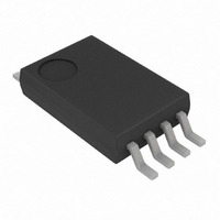
MCP6022T-I/ST Microchip Technology, MCP6022T-I/ST Datasheet - Page 19

MCP6022T-I/ST
Manufacturer Part Number
MCP6022T-I/ST
Description
IC OPAMP 2.5V DUAL R-R 8TSSOP
Manufacturer
Microchip Technology
Datasheet
1.MCP6021-ESN.pdf
(42 pages)
Specifications of MCP6022T-I/ST
Amplifier Type
General Purpose
Number Of Circuits
2
Output Type
Rail-to-Rail
Slew Rate
7 V/µs
Gain Bandwidth Product
10MHz
Current - Input Bias
1pA
Voltage - Input Offset
500µV
Current - Supply
1mA
Current - Output / Channel
30mA
Voltage - Supply, Single/dual (±)
2.5 V ~ 5.5 V
Operating Temperature
-40°C ~ 85°C
Mounting Type
Surface Mount
Package / Case
8-TSSOP
Lead Free Status / RoHS Status
Lead free / RoHS Compliant
-3db Bandwidth
-
Other names
MCP6022TI/ST
Available stocks
Company
Part Number
Manufacturer
Quantity
Price
Part Number:
MCP6022T-I/ST
Manufacturer:
MICROCHIP/微芯
Quantity:
20 000
4.6
The single op amps (MCP6021 and MCP6023), not in
the SOT-23-5 package, have an internal mid-supply
reference voltage connected to the V
Figure
V
provides a mid-supply reference. With the MCP6023,
taking the CS pin high conserves power by shutting
down both the op amp and the V
the CS pin low turns on the op amp and V
FIGURE 4-7:
circuit (MCP6021 and MCP6023 only).
See
internal
capacitor (C
amp input to the source.
FIGURE 4-8:
using V
To use the internal mid-supply reference for an
inverting gain circuit, connect the V
non-inverting input, as shown in
capacitor C
output.
© 2009 Microchip Technology Inc.
SS
, which always keeps the op amp on and always
Figure 4-8
4-7). The MCP6021 has CS internally tied to
V
(CS tied internally to V
REF
IN
MCP6021 and MCP6023 Reference
Voltage
mid-supply
B
V
B
(MCP6021 and MCP6023 only).
REF
) also reduces noise by coupling the op
helps reduce power supply noise on the
CS
for a non-inverting gain circuit using the
R
C
G
B
Simplified internal V
Non-inverting gain circuit
5 MΩ
reference.
R
SS
V
F
REF
V
V
for MCP6021)
DD
SS
REF
The
50 kΩ
50 kΩ
Figure
circuitry. Taking
REF
REF
REF
V
DC-blocking
OUT
pin to the
REF
4-9. The
pin (see
circuitry.
FIGURE 4-9:
V
If you don’t need the mid-supply reference, leave the
V
4.7
With this family of operational amplifiers, the power
supply pin (V
bypass capacitor (i.e., 0.01 µF to 0.1 µF) within 2 mm
for good, high-frequency performance. It also needs a
bulk capacitor (i.e., 1 µF or larger) within 100 mm to
provide large, slow currents. This bulk capacitor can be
shared with nearby analog parts.
4.8
An unused op amp in a quad package (MCP6024)
should be configured as shown in
circuits prevent the output from toggling and causing
crosstalk. Circuits A sets the op amp at its minimum
noise gain. The resistor divider produces any desired
reference voltage within the output voltage range of the
op amp; the op amp buffers that reference voltage.
Circuit B uses the minimum number of components
and operates as a comparator, but it may draw more
current.
FIGURE 4-10:
REF
REF
V
DD
¼ MCP6024 (A)
V
REF
R
R
pin open.
(MCP6021 and MCP6023 only).
V
MCP6021/1R/2/3/4
1
2
IN
Supply Bypass
Unused Op Amps
=
V
DD
DD
V
DD
R
for single supply) should have a local
×
G
------------------ -
R
1
R
+
Inverting gain circuit using
Unused Op Amps.
2
R
V
2
REF
R
F
V
C
REF
B
Figure
¼ MCP6024 (B)
DS21685D-page 19
4-10. These
V
V
OUT
DD


