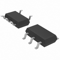
LT1782CS5#TRM Linear Technology, LT1782CS5#TRM Datasheet - Page 11

LT1782CS5#TRM
Manufacturer Part Number
LT1782CS5#TRM
Description
IC OPAMP R-R IN/OUT TSOT-23-5
Manufacturer
Linear Technology
Series
Over-The-Top®r
Datasheet
1.LT1782IS5TRMPBF.pdf
(16 pages)
Specifications of LT1782CS5#TRM
Amplifier Type
General Purpose
Number Of Circuits
1
Output Type
Rail-to-Rail
Slew Rate
0.075 V/µs
Gain Bandwidth Product
225kHz
Current - Input Bias
8nA
Voltage - Input Offset
500µV
Current - Supply
45µA
Current - Output / Channel
30mA
Voltage - Supply, Single/dual (±)
2.5 V ~ 18 V, ±1.25 V ~ 9 V
Operating Temperature
0°C ~ 70°C
Mounting Type
Surface Mount
Package / Case
TSOT-23-5, TSOT-5, TSOP-5
Lead Free Status / RoHS Status
Contains lead / RoHS non-compliant
-3db Bandwidth
-
Other names
LT1782CS5
LT1782CS5
Q1158155
LT1782CS5
Q1158155
Available stocks
Company
Part Number
Manufacturer
Quantity
Price
TYPICAL PERFORMANCE CHARACTERISTICS
APPLICATIONS INFORMATION
Supply Voltage
The positive supply pin of the LT1782 should be bypassed
with a small capacitor (typically 0.1µF) within an inch of
the pin. When driving heavy loads, an additional 4.7µF
electrolytic capacitor should be used. When using split
supplies, the same is true for the negative supply pin.
The LT1782 is protected against reverse battery voltages
up to 18V. In the event a reverse battery condition occurs,
the supply current is typically less than 1nA.
Inputs
The LT1782 has two input stages, NPN and PNP (see the
Simplified Schematic), resulting in three distinct operating
regions as shown in the Input Bias Current vs Common
Mode typical performance curve.
For input voltages about 0.8V or more below V
input stage is active and the input bias current is typically
–8nA. When the input common mode voltage is within
0.5V of the positive rail, the NPN stage is operating and
the input bias current is typically 15nA. Increases in tem-
perature will cause the voltage at which operation switches
from the PNP input stage to the NPN input stage to move
towards V
untrimmed and is typically 1.8mV.
50
40
30
20
10
0
0
Supply Current
vs Shutdown Voltage
+
. The input offset voltage of the NPN stage is
0.5
SHUTDOWN PIN VOLTAGE (V)
T
A
= 125°C
T
1
A
= 25°C
T
A
1.5
= –55°C
V
S
2
= 5V, 0V
1782 G28
2.5
Large-Signal Response
+
V
A
C
, the PNP
S
V
L
= ±5V
= 1
= 15pF
A Schottky diode in the collector of the input NPN tran-
sistors, along with special geometries for these NPN
transistors, allows the LT1782 to operate with either or
both of its inputs above V
NPN input transistor is fully saturated and the input bias
current is typically 4µA at room temperature. The input
offset voltage is typically 1.8mV when operating above
V
V
The inputs are protected against excursions as much as
10V below V
input and a diode from the input to the negative supply.
The input stage of the LT1782 incorporates phase reversal
protection to prevent the output from phase reversing for
inputs up to 9V below V
between the inputs and the maximum differential input
voltage is 18V.
Output
The output of the LT1782 can swing to within 60mV of the
positive rail with no load and within 3mV of the negative
rail with no load. When monitoring voltages within 60mV
of the positive rail or within 3mV of the negative rail, gain
should be taken to keep the output from clipping. The
LT1782 can sink and source over 30mA at ±5V supplies,
+
–
. The LT1782 will operate with its inputs 18V above
regardless of V
1782 G29
–
by an internal 6k resistor in series with each
+
.
–
Small-Signal Response
. There are no clamping diodes
V
A
C
+
S
V
L
. At about 0.3V above V
= 15pF
= ±5V
= 1
LT1782
11
+
1782 G30
, the
1782fc


