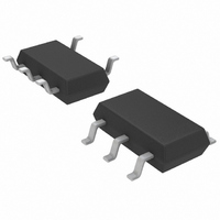
LT6220CS5#TRM Linear Technology, LT6220CS5#TRM Datasheet - Page 13

LT6220CS5#TRM
Manufacturer Part Number
LT6220CS5#TRM
Description
IC OPAMP PREC LP R-R TSOT23-5
Manufacturer
Linear Technology
Datasheet
1.LT6220CS5TRMPBF.pdf
(20 pages)
Specifications of LT6220CS5#TRM
Amplifier Type
General Purpose
Number Of Circuits
1
Output Type
Rail-to-Rail
Slew Rate
20 V/µs
Gain Bandwidth Product
60MHz
Current - Input Bias
250nA
Voltage - Input Offset
700µV
Current - Supply
1mA
Current - Output / Channel
50mA
Voltage - Supply, Single/dual (±)
2.2 V ~ 12.6 V, ±1.1 V ~ 6.3 V
Operating Temperature
0°C ~ 70°C
Mounting Type
Surface Mount
Package / Case
TSOT-23-5, TSOT-5, TSOP-5
Lead Free Status / RoHS Status
Contains lead / RoHS non-compliant
-3db Bandwidth
-
Other names
LT6220CS5#TRMTR
Available stocks
Company
Part Number
Manufacturer
Quantity
Price
APPLICATIO S I FOR ATIO
Circuit Description
The LT6220/LT6221/LT6222 have an input and output
signal range that covers from the negative power supply to
the positive power supply. Figure 1 depicts a simplified
schematic of the amplifier. The input stage comprises two
differential amplifiers, a PNP stage, Q1/Q2, and an NPN
stage, Q3/Q4, that are active over different ranges of
common mode input voltage. The PNP stage is active
between the negative supply to approximately 1.2V below
the positive supply. As the input voltage moves closer
toward the positive supply, the transistor Q5 will steer the
2V/DIV
TYPICAL PERFOR A CE CHARACTERISTICS
0V
V
V
±5V Large-Signal Response
V
A
R
+
–
S
V
L
= ±5V
= 1
= 1k
Q16
+
I
2
+IN
–IN
Q17
200ns/DIV
U
Q18
ESDD1
ESDD4
U
W
V
V
–
+
622012 G38
Figure 1. LT6220/LT6221/LT6222 Simplified Schematic Diagram
V
V
–
+
U
ESDD2
ESDD3
W
D6
D5
50mV/DIV
D8
D7
Q19
0V
U
±5V Small-Signal Response
V
A
R
S
V
L
Q4
= ±5V
= 1
= 1k
Q7
D1
D2
Q3
Q5
Q6
50ns/DIV
tail current, I
NPN differential pair and the PNP pair becomes inactive
for the rest of the input common mode range up to the
positive supply. Also, at the input stage, devices Q17 to
Q19 act to cancel the bias current of the PNP input pair.
When Q1/Q2 are active, the current in Q16 is controlled to
be the same as the current Q1/Q2. Thus, the base current
of Q16 is nominally equal to the base current of the input
devices. The base current of Q16 is then mirrored by
devices Q17-Q19 to cancel the base current of the input
devices Q1/Q2.
V
BIAS
Q1
+
D3
D4
Q2
I
1
622012 G39
LT6220/LT6221/LT6222
1
, to the current mirror, Q6/Q7, activating the
Q10
Q11
Q9
1V/DIV
2V/DIV
R3
R1
V
OUT
V
Q12
0V
0V
IN
Output Overdriven Recovery
V
A
R
Q8
S
V
L
R4
R2
= 5V, 0V
= 2
= 1k
C
C
+
V
Q13
OUTPUT BIAS
–
R5
BUFFER
I
3
AND
200ns/DIV
C2
C1
622012 F01
Q15
Q14
13
OUT
622012fa
622012 G40


