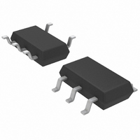
LTC2050HVHS5#TRPBF Linear Technology, LTC2050HVHS5#TRPBF Datasheet - Page 6

LTC2050HVHS5#TRPBF
Manufacturer Part Number
LTC2050HVHS5#TRPBF
Description
IC OPAMP ZERO-DRIFT TSOT23-5
Manufacturer
Linear Technology
Datasheet
1.LTC2050CS5TRMPBF.pdf
(16 pages)
Specifications of LTC2050HVHS5#TRPBF
Amplifier Type
Chopper (Zero-Drift)
Number Of Circuits
1
Output Type
Rail-to-Rail
Slew Rate
2 V/µs
Gain Bandwidth Product
3MHz
Current - Input Bias
25pA
Voltage - Input Offset
0.5µV
Current - Supply
1mA
Voltage - Supply, Single/dual (±)
2.7 V ~ 11 V, ±1.35 V ~ 5.5 V
Operating Temperature
-40°C ~ 125°C
Mounting Type
Surface Mount
Package / Case
TSOT-23-5, TSOT-5, TSOP-5
Lead Free Status / RoHS Status
Lead free / RoHS Compliant
Current - Output / Channel
-
-3db Bandwidth
-
Available stocks
Company
Part Number
Manufacturer
Quantity
Price
Part Number:
LTC2050HVHS5#TRPBFLTC2050HVHS5#TRMPBF
Manufacturer:
LINEAR/凌特
Quantity:
20 000
ELECTRICAL CHARACTERISTICS
LTC2050/LTC2050HV
operating temperature range, otherwise specifi cations are at T
Note 1: Stresses beyond those listed under Absolute Maximum Ratings
may cause permanent damage to the device. Exposure to any Absolute
Maximum Rating condition for extended periods may affect device
reliability and lifetime.
Note 2: These parameters are guaranteed by design. Thermocouple effects
preclude measurements of these voltage levels during automated testing.
Note 3: All versions of the LTC2050 are designed, characterized and
expected to meet the extended temperature limits of – 40°C and 125°C.
PARAMETER
Input Offset Voltage
Average Input Offset Drift
Long-Term Offset Drift
Input Bias Current (Note 4)
Input Offset Current (Note 4)
Input Noise Voltage
Common Mode Rejection Ratio
Power Supply Rejection Ratio
Large-Signal Voltage Gain
Maximum Output Voltage Swing
Slew Rate
Gain Bandwidth Product
Supply Current
Shutdown Pin Input Low Voltage (V
Shutdown Pin Input High Voltage (V
Shutdown Pin Input Current
Internal Sampling Frequency
6
IL
IH
)
)
CONDITIONS
(Note 2)
(Note 2)
R
V
V
V
R
R
R
V
V
V
CM
CM
S
SHDN
SHDN
SHDN
S
L
L
L
= 2.7V to 11V
= 10k
= 2k to GND
= 10k to GND
= 100Ω, 0.01Hz to 10Hz
= V
= V
= V
= V
= V
–
–
to (V
to (V
IH
IL
–
, No Load
+
+
– 1.3)
– 1.3)
(LTC2050HV) The
A
l
l
l
l
l
l
l
l
l
l
l
l
= 25°C. V
V
±4.75
±4.90
+
MIN
120
115
120
115
125
120
– 0.5
The LTC2050C/LTC2050HVC are guaranteed to meet the temperature limits
of 0°C and 70°C. The LTC2050I/LTC2050HVI are guaranteed to meet the
temperature limits of –40°C and 85°C. The LTC2050H/LTC2050HVH are
guaranteed to meet the temperature limits of –40°C and 125°C.
Note 4: The bias current measurement accuracy depends on the proximity
of the supply bypass capacitor to the device under test, especially at ±5V
supplies. Because of testing limitations on the placement of this bypass
capacitor, the bias current at ±5V supplies is guaranteed by design to meet
the data sheet limits, but tested to relaxed limits.
S
C, I SUFFIXES
= ±5V unless otherwise noted. (Note 3)
l
±4.94
±4.98
denotes the specifi cations which apply over the full
±0.5
TYP
±25
130
130
130
130
140
140
1.5
7.5
50
–3
2
3
1
V
±0.03
±125
±300
±250
±500
–
MAX
–20
1.5
±3
25
+ 0.5
V
±4.50
±4.85
+
MIN
120
115
120
115
125
120
– 0.5
H SUFFIX
±4.94
±4.98
±0.5
TYP
±25
130
130
130
130
140
140
1.5
7.5
50
–3
2
3
1
V
±4000
±1000
±0.05
±125
±250
–
MAX
–20
1.6
±3
25
+ 0.5
nV/√mo
UNITS
μV/°C
μV
2050fc
V/μs
MHz
kHz
mA
P-P
pA
pA
pA
pA
dB
dB
dB
dB
dB
dB
μA
μV
μA
V
V
V
V


